Pin description – Rainbow Electronics MAX9486 User Manual
Page 5
MAX9486
8kHz Reference Clock Synthesizer
with Multiple Outputs at 35.328MHz
_______________________________________________________________________________________
5
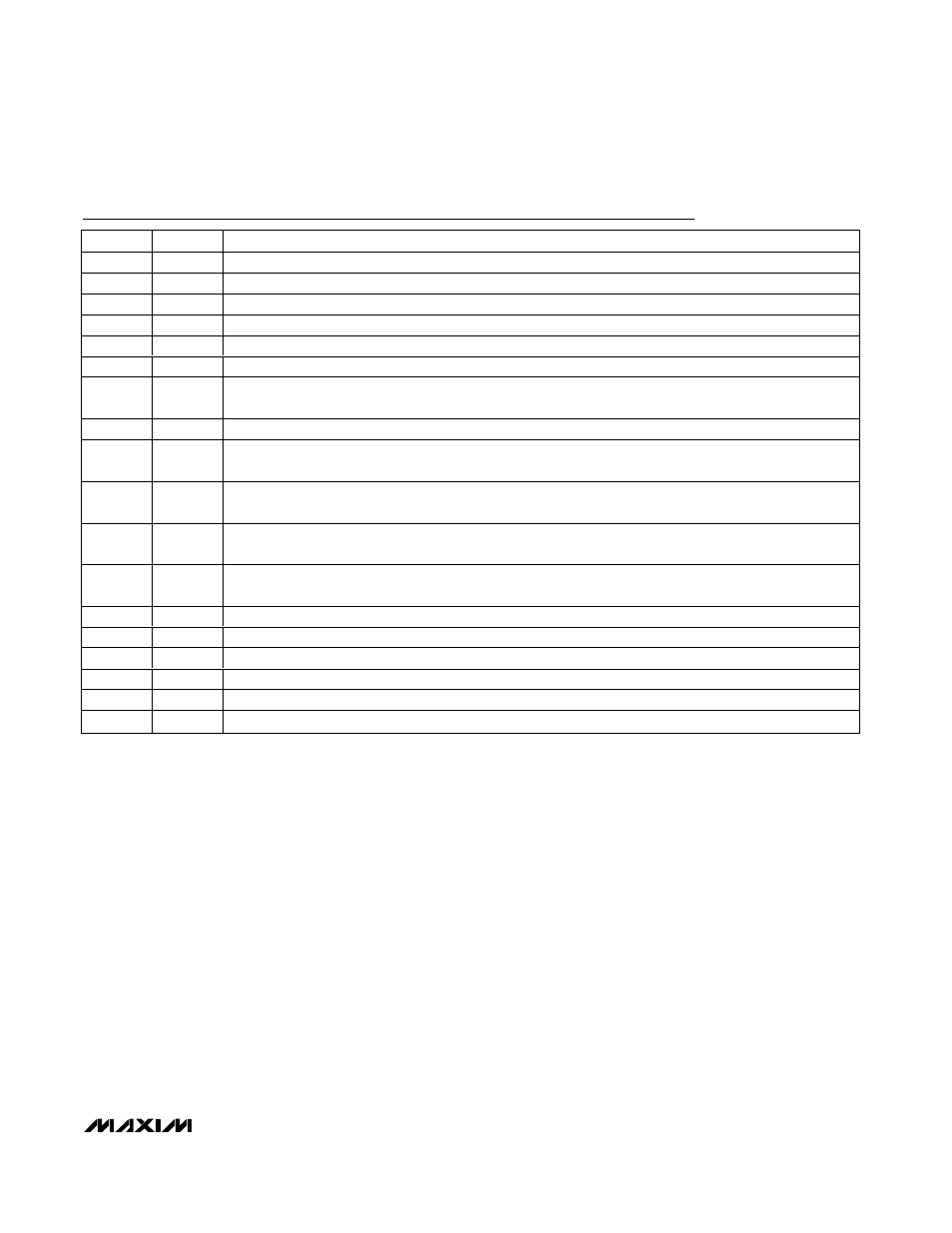
PIN
NAME
FUNCTION
1
SHDN
Active-Low Shutdown Input
2
REO
Reference Clock Output. REO is an 8kHz reference clock output with jitter suppression.
3
REIN
Reference Input
4
V
DDP
Phase-Lock Loop (PLL) Power Supply. Bypass V
DDP
with 0.1µF and 0.001µF capacitors to GNDP.
5
GNDP
PLL Ground
6
X1
Crystal Input 1. Connect X1 to a fundamental mode crystal for the VCXO.
7, 16, 19,
21
V
DD
Digital Power Supply. Bypass V
DD
with 0.1µF and 0.001µF capacitors to GND.
8
X2
Crystal Input 2. Connect X2 to a fundamental mode crystal for the VCXO.
9, 14, 18,
23
GND
Ground
10
LP2
External Filter 2. Connect the loop filter capacitors and a resistor between LP1 and LP2 (see the Typical
Application Circuit). LP2 is internally connected to GNDP.
11
LP1
External Filter 1. Connect the loop filter capacitors and a resistor between LP1 and LP2 (see the Typical
Application Circuit).
12
SETI
Charge-Pump Current-Setting Input. Connect a resistor from SETI to GNDP to set PLL charge-pump current
(see the Detailed Description section).
13
CLK6
Clock Output 6 at 35.328MHz
15
CLK5
Clock Output 5 at 35.328MHz
17
CLK4
Clock Output 4 at 35.328MHz
20
CLK3
Clock Output 3 at 35.328MHz
22
CLK2
Clock Output 2 at 35.328MHz
24
CLK1
Clock Output 1 at 35.328MHz
Pin Description