Programmable pre-amplifier, Interface, Programmable gain – Xilinx MIcroblaze Development Spartan-3E 1600E User Manual
Page 79
MicroBlaze Development Kit Spartan-3E 1600 Edition User Guide
77
UG257 (v1.1) December 5, 2007
Programmable Pre-Amplifier
R
The reference design files provide more information on converting the voltage applied on
VINA or VINB to a digital representation (see
).
Programmable Pre-Amplifier
The LTC6912-1 provides two independent inverting amplifiers with programmable gain.
The purpose of the amplifier is to scale the incoming voltage on VINA or VINB so that it
maximizes the conversion range of the DAC, namely 1.65 r 1.25V.
Interface
Table 10-1
lists the interface signals between the FPGA and the amplifier. The SPI_MOSI,
SPI_MISO, and SPI_SCK signals are shared with other devices on the SPI bus. The
AMP_CS signal is the active-Low slave select input to the amplifier.
Programmable Gain
Each analog channel has an associated programmable gain amplifier (see
Analog signals presented on the VINA or VINB inputs on header J7 are amplified relative
to 1.65V. The 1.65V reference is generated using a voltage divider of the 3.3V voltage
supply.
The gain of each amplifier is programmable from -1 to -100, as shown in
Table 10-2
.
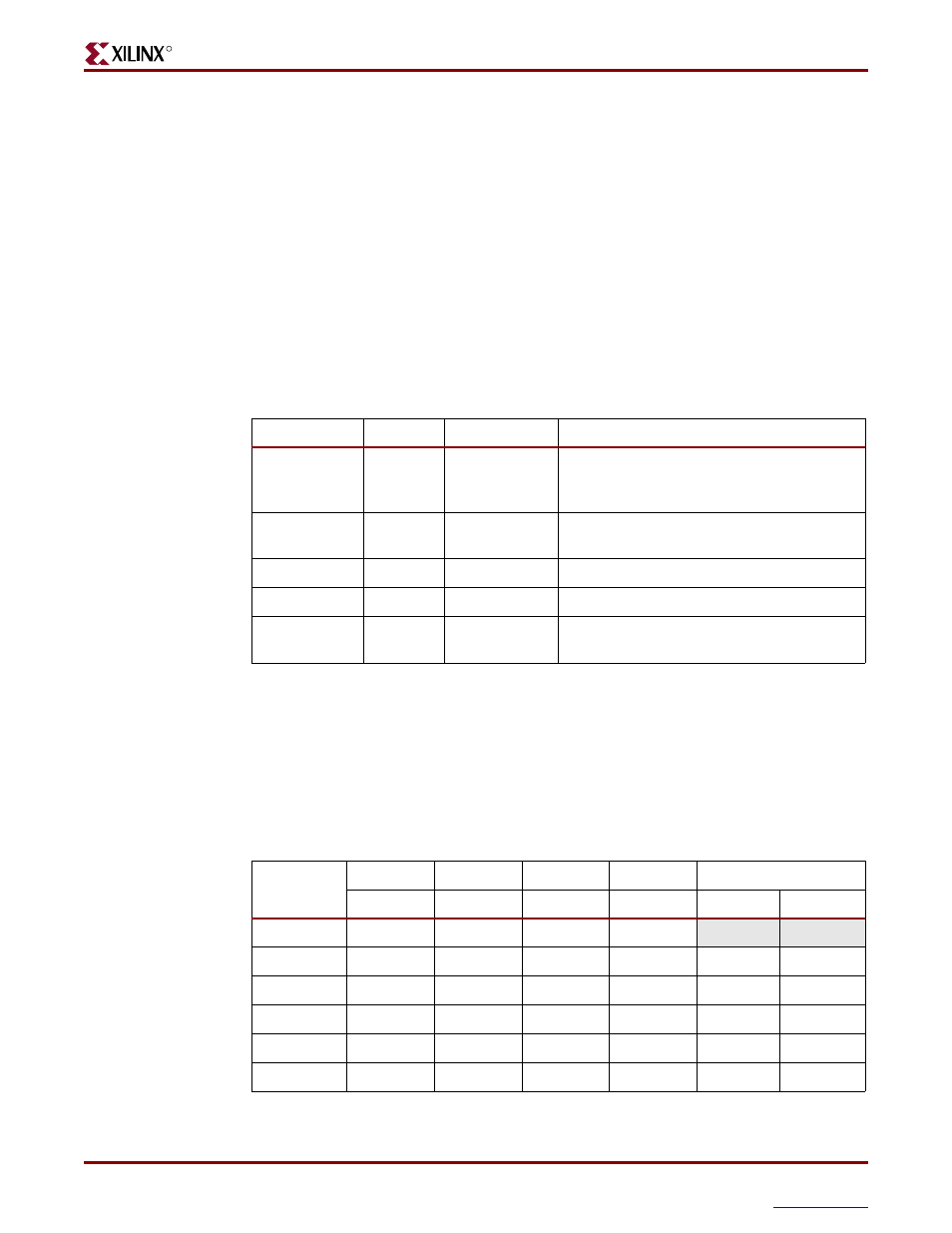
Table 10-1:
AMP Interface Signals
Signal
FPGA Pin
Direction
Description
SPI_MOSI
T4
FPGAÆAD
Serial data: Master Output, Slave Input.
Presents 8-bit programmable gain settings, as
defined in
Table 10-2
.
AMP_CS
N7
FPGAÆAMP
Active-Low chip-select. The amplifier gain is
set when signal returns High.
SPI_SCK
U16
FPGAÆAMP
Clock
AMP_SHDN
P7
FPGAÆAMP
Active-High shutdown, reset
AMP_DOUT
E18
FPGAÅAMP
Serial data. Echoes previous amplifier gain
settings. Can be ignored in most applications.
Table 10-2:
Programmable Gain Settings for Pre-Amplifier
Gain
A3
A2
A1
A0
Input Voltage Range
B3
B2
B1
B0
Minimum
Maximum
0
0
0
0
0
-1
0
0
0
1
0.4
2.9
-2
0
0
1
0
1.025
2.275
-5
0
0
1
1
1.4
1.9
-10
0
1
0
0
1.525
1.775
-20
0
1
0
1
1.5875
1.7125