Using differential inputs – Xilinx MIcroblaze Development Spartan-3E 1600E User Manual
Page 122
120
MicroBlaze Development Kit Spartan-3E 1600 Edition User Guide
UG257 (v1.1) December 5, 2007
Chapter 15:
Expansion Connectors
R
Using Differential Inputs
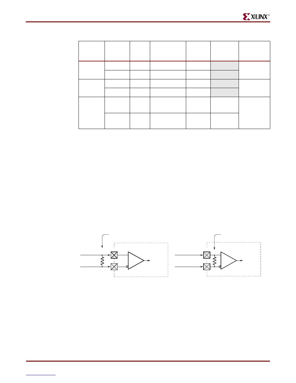
LVDS and RSDS differential inputs require input termination. Two options are available.
The first option is to use external termination resistors, as shown in
Figure 15-3a
. The
board provides landing pads for external 100: termination resistors. The resistors are not
loaded on the board as shipped. The resistor reference designators are labeled on the
silkscreen, as listed in
The landing pads are located on both the top- and
bottom-side of the board, between the FPGA and the FX2 connector. The resistors are not
loaded on the board as shipped. External termination is always required when using
differential input pairs 15 and 16.
The second option, shown in
Figure 15-3b
, is a Spartan-3E feature called on-chip
differential termination, which uses the DIFF_TERM attribute available on differential I/O
signals. Each differential I/O pin includes a circuit that behaves like an internal
termination resistor of approximately 120:. On-chip differential termination is only
available on I/O pairs, not on Input-only pairs like pairs 15 and 16 in
.
Figure 15-4
and
Figure 15-5
show the locations of the differential input termination resistor
landing pads on the top and bottom side of the board.
indicates which resistor is
associated with a specific differential pair.
15
FX2_IP35
D12
IP_L07N_0
Input
R208
FX2_IP36
C12
IP_L07P_0
Input
16
FX2_IP37
A15
IP_L02N_0
Input
R209
FX2_IP38
B15
IP_L02P_0
Input
17
FX2_
CLKIN
E10
IO_L11N_0/
GCLK5
I/O
Yes
R210
FX2_
CLKOUT
D10
IO_L11P_0/
GCLK4
I/O
Yes
Table 15-2:
Differential I/O Pairs (Continued)
Differential
Pair
Signal
Name
FPGA
Pins
FPGA Pin Name Direction DIFF_TERM
External
Resistor
Designator
Figure 15-3:
Differential Input Termination Options
LxxN_0
LxxP_0
Signal
LxxN_0
LxxP_0
Signal
Pads for 100
Ω
surface-mount resistor
Differential termination
(~120
Ω)
a) External 100W termination resistor
b) On-chip differential termination
FPGA
FPGA
PAD
PAD
UG257_15_03_060806