Digital to analog converter (dac), Spi communication, Chapter 9: digital to analog converter (dac) – Xilinx MIcroblaze Development Spartan-3E 1600E User Manual
Page 71: Chapter 9, “digital to analog converter (dac), Chapter 9
MicroBlaze Development Kit Spartan-3E 1600 Edition User Guide
69
UG257 (v1.1) December 5, 2007
R
Chapter 9
Digital to Analog Converter (DAC)
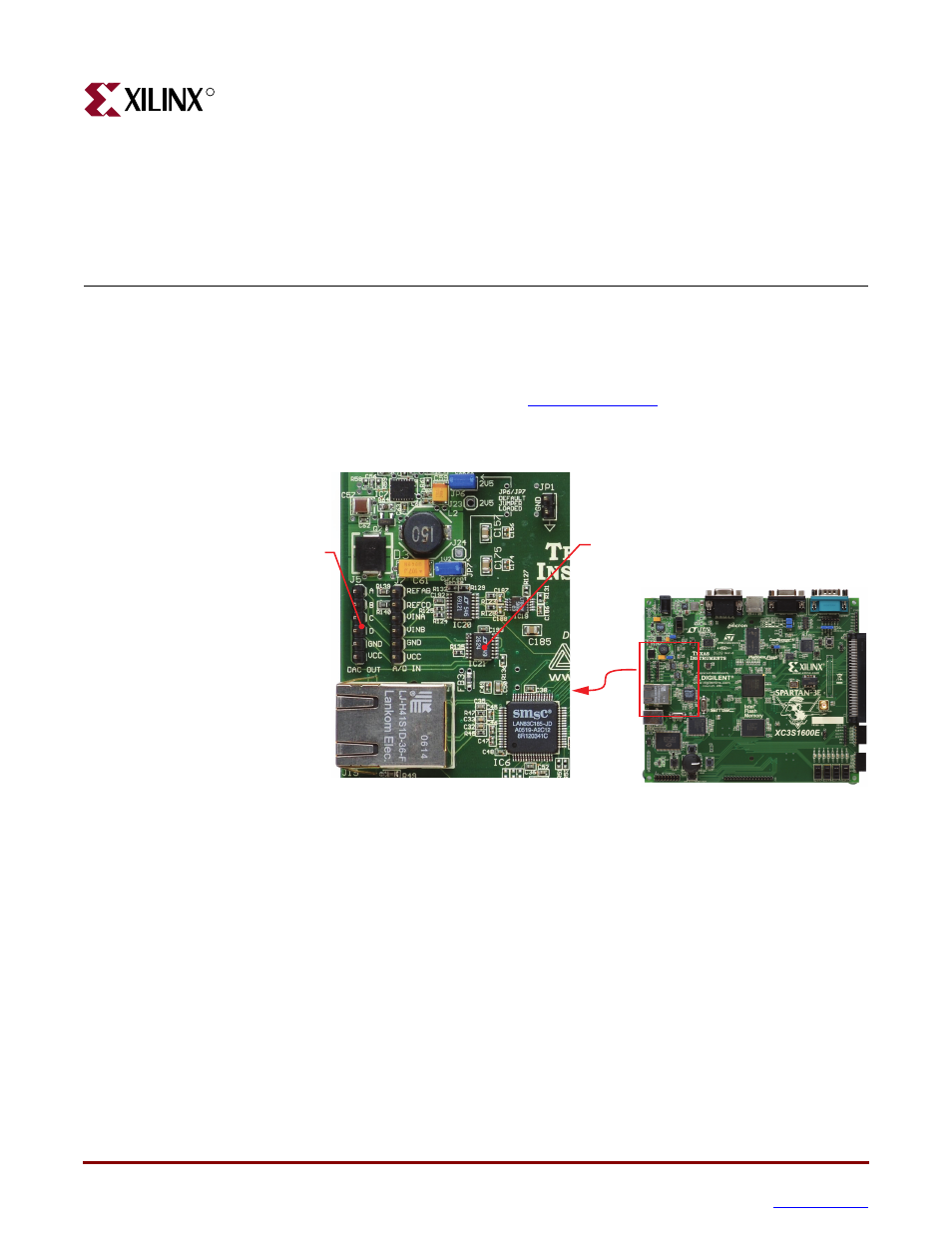
The MicroBlaze Development Kit board includes an SPI-compatible, four-channel, serial
Digital-to-Analog Converter (DAC). The DAC device is a Linear Technology LTC2624
quad DAC with 12-bit unsigned resolution. The four outputs from the DAC appear on the
J5 header, which uses the Digilent
format. The DAC and the
header are located immediately above the Ethernet RJ-45 connector, as shown in
SPI Communication
As shown in
Figure 9-2
, the FPGA uses a Serial Peripheral Interface (SPI) to communicate
digital values to each of the four DAC channels. The SPI bus is a full-duplex, synchronous,
character-oriented channel employing a simple four-wire interface. A bus master—the
FPGA in this example—drives the bus clock signal (SPI_SCK) and transmits serial data
(SPI_MOSI) to the selected bus slave—the DAC in this example. At the same time, the bus
slave provides serial data (SPI_MISO) back to the bus master.
Figure 9-1:
Digital-to-Analog Converter and Associated Header
Linear Tech LTC2624 Quad DAC
SPI_MOSI: (T4)
SPI_MISO: (N10)
SPI_SCK: (U16)
DAC_CS: (N8)
DAC_CLR: (P8)
Spartan-3E
Development Board
UG257_04_01_061306
6-pin DAC
Header (J5)