Specifying the dac output voltage, Dac outputs a and b, Figure 9-4 – Xilinx MIcroblaze Development Spartan-3E 1600E User Manual
Page 74
72
MicroBlaze Development Kit Spartan-3E 1600 Edition User Guide
UG257 (v1.1) December 5, 2007
Chapter 9:
Digital to Analog Converter (DAC)
R
master. The response from the DAC can be ignored although it is a useful to confirm
correct communication.
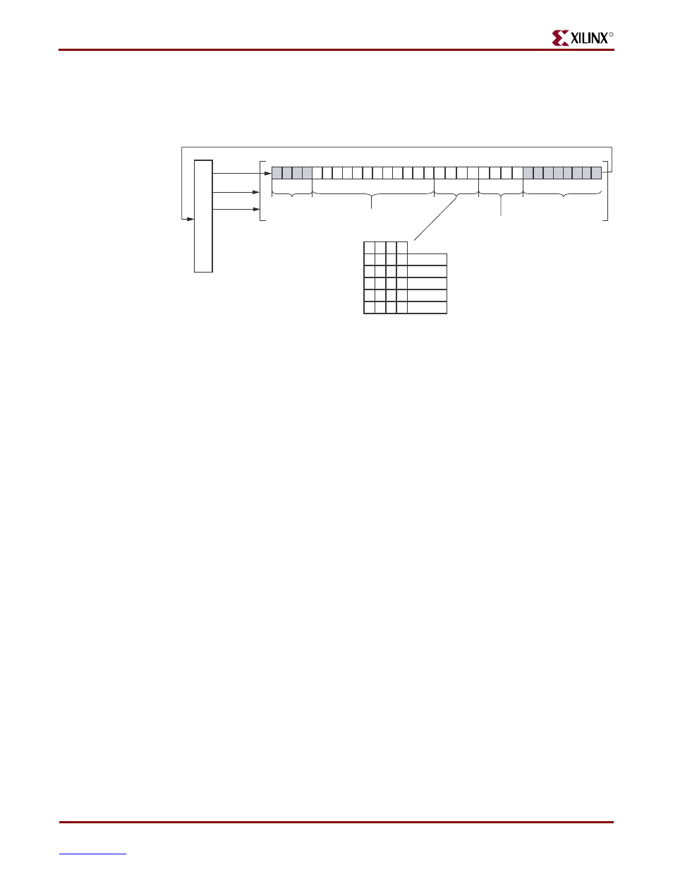
The FPGA first sends eight dummy or “don’t care” bits, followed by a 4-bit command. The
most commonly used command with the board is COMMAND[3:0] = “0011”, which
immediately updates the selected DAC output with the specified data value. Following the
command, the FPGA selects one or all the DAC output channels via a 4-bit address field.
Following the address field, the FPGA sends a 12-bit unsigned data value that the DAC
converts to an analog value on the selected output(s). Finally, four additional dummy or
don’t care
bits pad the 32-bit command word.
Specifying the DAC Output Voltage
As shown in
Figure 9-2
, each DAC output level is the analog equivalent of a 12-bit
unsigned digital value, D[11:0], written by the FPGA to the DAC via the SPI interface.
The voltage on a specific output is generally described in
. The reference
voltage, V
REFERENCE
, is different between the four DAC outputs. Channels A and B use a
3.3V reference voltage and Channels C and D use a 2.5V reference. The reference voltages
themselves have a r5% tolerance, so there will be slight corresponding variances in the
output voltage.
Equation 9-1
DAC Outputs A and B
provides the output voltage equation for DAC outputs A and B. The
reference voltage associated with DAC outputs A and B is 3.3V r 5%.
Equation 9-2
Figure 9-4:
SPI Communications Protocol to LTC2624 DAC
0
31
x x
x x
x x
x x
x x
x x
9 10 11
8
7
6
5
4
3
2
1
0
ADDRESS
a3
a2
a1
a0
a
3
a
2
a
1
a
0
c3
c2
c1
c0
0 0 0 0
0 0 0 1
0 0 1 0
0 0 1 1
All
DAC A
DAC B
DAC C
DAC D
1 1 1 1
SPI_MOSI
SPI_SCK
DAC_CS
SPI_MISO
12-bit Unsigned
DATA
COMMAND
Don’t Care
UG257_09_04_060606
msb
lsb
Don’t Care
Slave: LTC2624 DAC
M
as
ter
S
pa
rt
an-
3E FPGA
V
OUT
D
11:0
>
@
4096
--------------------- V
REFERENCE
u
=
V
OUTA
D
11:0
>
@
4096
---------------------
3.3V 5%
r
u
=