2functional description, 1 analog processing and a/d converters, 1 video input switch control – Texas Instruments TVP5147M1PFP User Manual
Page 17

Functional Description
9
SLES140A—March 2007
TVP5147M1PFP
2
Functional Description
2.1
Analog Processing and A/D Converters
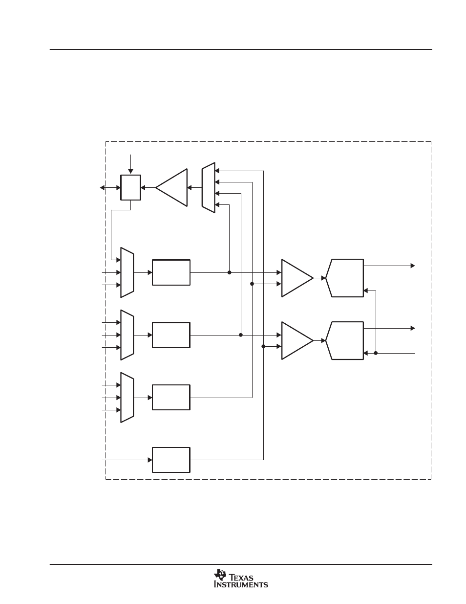
Figure 2−1 shows a functional diagram of the analog processors and A/D converters, which provide the analog
interface to all video inputs. It accepts up to 10 inputs and performs source selection, video clamping, video
amplification, A/D conversion, and gain and offset adjustments to center the digitized video signal. The
TVP5147M1 supports one analog video output for the selected analog input video.
Clamp
CH1 A/D
Line-Locked
Sampling Clock
VI_4_A
M
U
X
VI_1_B
VI_1_C
M
U
X
VI_2_A
VI_2_B
VI_2_C
M
U
X
VI_3_A
VI_3_B
VI_3_C
11-Bit
ADC
Clamp
Clamp
Clamp
VI_1_A
I/O
PGA
CVBS/
Pb/C
CVBS/
Y
CVBS/
Pr/C
CVBS/
Y
M
U
X
PGA
CH2 A/D
11-Bit
ADC
PGA
Analog Front End
Figure 2−1. Analog Processors and A/D Converters
2.1.1 Video Input Switch Control
The TVP5147M1 decoder has two analog channels that accept up to 10 video inputs. The user can configure
the internal analog video switches via the I
2
C interface. The 10 analog video inputs can be used for different
input configurations, some of which are:
