Figure 3-7 – Texas Instruments TMS320F2802 User Manual
Page 42

XINT2
C28x
CPU
CPU TIMER 2 (Reserved for DSP/BIOS)
CPU TIMER 0
Watchdog
Peripherals
(SPI, SCI, I2C, eCAN, ePWM, eCAP, eQEP, ADC)
TINT0
Interrupt Control
XNMICR(15:0)
XINT1
MUX
MUX
MUX
MUX
MUX
Interrupt Control
XINT1
XINT1CR(15:0)
Interrupt Control
XINT2
96 Interrupts
PIE
XINT2CR(15:0)
GPIO
MUX
WDINT
INT1
to
INT12
INT13
INT14
NMI
XINT1CTR(15:0)
XINT2CTR(15:0)
XNMICTR(15:0)
CPU TIMER 1
TINT2
Low-Power Modes
LPMINT
WAKEINT
TINT1
int13_select
XNMI_XINT13
GPIO0.int
GPIO31.int
ADC
XINT2SOC
GPIOXINT1SEL(4:0)
GPIOXINT2SEL(4:0)
GPIOXNMISEL(4:0)
nmi_select
1
, , ,
SPRS230N – OCTOBER 2003 – REVISED MAY 2012
When the PIE is enabled, TRAP #1 through TRAP #12 will transfer program control to the interrupt service
routine corresponding to the first vector within the PIE group. For example: TRAP #1 fetches the vector
from INT1.1, TRAP #2 fetches the vector from INT2.1 and so forth.
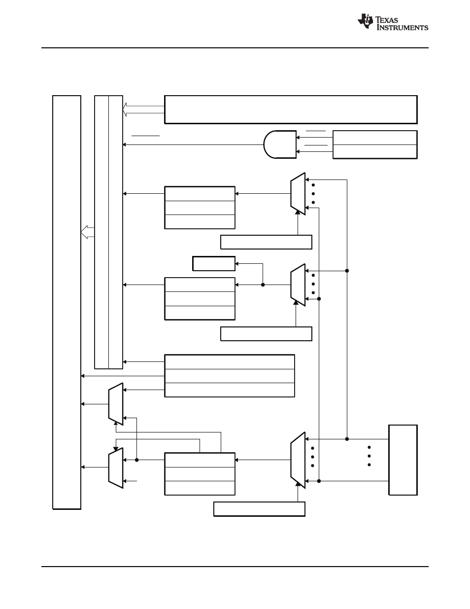
Figure 3-7. External and PIE Interrupt Sources
42
Functional Overview
Copyright © 2003–2012, Texas Instruments Incorporated
Product Folder Link(s):
