Bt8960 – Rockwell SoniCrafter BT8960 User Manual
Page 97
87
4.0 Electrical & Mechanical Specifications
4.6 Microcomputer Interface Timing
Bt8960
Single-Chip 2B1Q Transceiver
N8960DSB
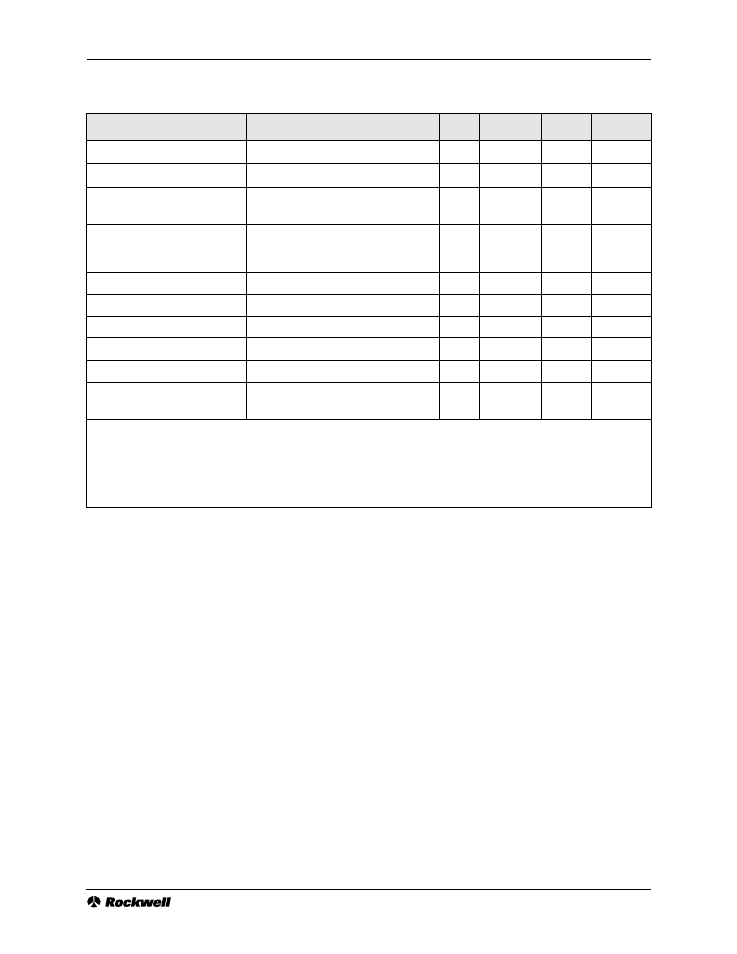
Table 4-18. Transmitter Analog Requirements and Specifications
Parameter
Comments
Min
Typ
Max
Units
Transmit Symbol Rate (f
qclk
)
QCLK Frequency (Data Rate/2)
75
210
kHz
Pulse Template
(1, 2,3)
See Figure 4-13, R
L
= 135
Ω
Average Power
(1, 2,4)
DC to 2xF
QCLK
, R
L
= 135
Ω
, 0dB gain
setting
13.4
14.0
dBm
Gain Adjustment Step
Controlled by Transmit Gain Register
[0x29]. Seven steps above and eight
steps below 0 dB.
0.17
0.20
0.24
dB
Output Referred Offset Voltage
25
mV
Output Current
125
mA
Common-Mode Voltage
VCOMO
VAA/2
V
Output Impedance
(1)
DC to 1 MHz
2
W
Linearity
At Output Symbol Peak
0.01
%FSR
(5)
Harmonic Distortion
3 kHz, 3.4 V Peak Sine Wave Output, R
L
= 0
Ω
–70
dB
Notes: (1). Guaranteed by design and characterization.
(2). See 4-14 of the Test Conditions section of this datasheet for test circuit.
(3). Measured after the transmitter is calibrated by writing the value in the Transmitter Calibration Register [tx_calibrate;
0x28] to the Transmitter Gain Register [tx_gain; 0x29].
(4). Measured with a pseudo-random code sequence of pulses.
(5). FSR is Full Scale Range.