Rockwell SoniCrafter BT8960 User Manual
Bt8960, Single-chip 2b1q transceiver

Bt8960
Single-Chip 2B1Q Transceiver
The Bt8960 is a full-duplex 2B1Q transceiver based on Rockwell’s HDSL technol-
ogy. It supports Nx64 kbps transmission of more than 18,000 feet
over 26 AWG
copper telephone wire without repeaters. Small size and low power dissipation
make the Bt8960 ideal for line-powered voice pairgain systems capable of provid-
ing four or six clear 64 kbps channels.
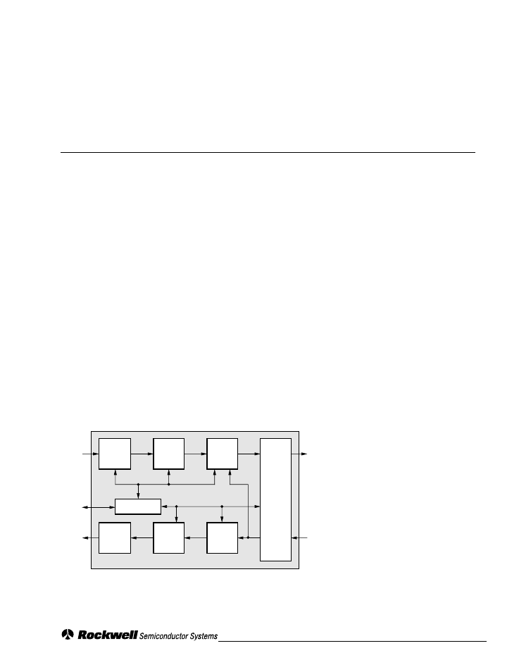
The Bt8960 is a highly integrated device that includes all of the active circuitry
needed for a complete 2B1Q transceiver. In the receive portion of the Bt8960, a
variable gain amplifier optimizes the signal level according to the dynamic range
of the analog-to-digital converter. Once the signal is digitized, sophisticated adap-
tive echo cancellation, equalization, and detection DSP algorithms reproduce the
originally transmitted far-end signal.
In the transmitter, the transmit source and scrambler operation is programma-
ble via the microcomputer interface. A highly linear digital-to-analog converter
with programmable gain, sets the transmission power for optimal performance. A
pulse-shaping filter and a low distortion line driver generate the signal character-
istics needed to drive a large range of subscriber lines at low-bit error rates.
Startup and performance monitoring operations are controlled via the micro-
processor interface. C-language source code supporting these operations is sup-
plied under a no-fee license agreement from Rockwell. The Bt8960 includes a
glueless interface to both Intel and Motorola microprocessors.
Functional Block Diagram
Distinguishing Features
•
Single-chip 2B1Q transceiver solution
•
All 2B1Q transceiver functions inte-
grated into a single monolithic device
– Receiver gain control and A/D
converter
– DSP functions including echo
cancellation, equalization, timing
recovery, and symbol detection
– Programmable gain transmit DAC,
pulse-shaping filter and line driver
•
Supports operation from 160 to 416
kbps
•
Capable of transceiving over the ANSI
T1.601 and ETSI ETR 080 ISDN
test loops
•
Flexible Monitoring and Control
– Glueless interface to Intel 8051 and
Motorola 68302 processors
– Access to embedded filters, perfor-
mance meters and timers
•
Backwards compatible with Bt8952
software API commands
•
JTAG/IEEE Std 1149.1-1990
compliant
•
Single +5 V power supply
operation
•
600 mW power consumption at 288
kbps (typical)
•
100-pin PQFP package
•
–40˚C to +85˚C operation
Applications
•
Voice/data pairgain systems
•
Internet connectivity
•
ISDN basic-rate interface
concentrators
•
ISDN H0 transport
•
Extended range fractional T1/E1
•
Cellular/microcellular base stations
•
Personal Communications Systems
(PCS) radio ports and cell switches
Analog
Receive
MPU
Bus
Analog
Transmit
Variable
Gain
Amplifier
Microcomputer
Interface
Line
Driver
Pulse-
Shaping
Filter
Program-
mable
Gain
DAC
Analog-
to-Digital
Converter
Digital
Signal
Processor
Framer/
Channel
Unit
Interface
Recovered
Data and
Clock
Transmit
Data
Document Outline
- Table of Contents
- 1.0 System Overview
- 2.0 Functional Description
- 2.1 Transmit Section
- 2.2 Receive Section
- 2.3 Timing Recovery and Clock Interface
- 2.4 Channel Unit Interface
- 2.5 Microcomputer Interface
- 2.6 Test and Diagnostic Interface (JTAG)
- 3.0 Registers
- 3.1 Conventions
- 3.2 Register Summary
- 3.2.1 0x00—Global Modes and Status Register (glo...
- 3.2.2 0x01—Serial Monitor Source Select Register...
- 3.2.3 0x02—Interrupt Mask Register Low (mask_low...
- 3.2.4 0x03—Interrupt Mask Register High (mask_hi...
- 3.2.5 0x04—Timer Source Register (timer_source)
- 3.2.6 0x05—IRQ Source Register (irq_source)
- 3.2.7 0x06—Channel Unit Interface Modes Register...
- 3.2.8 0x07—Receive Phase Select Register (receiv...
- 3.2.9 0x08—Linear Echo Canceller Modes Register ...
- 3.2.10 0x09—Nonlinear Echo Canceller Modes Regis...
- 3.2.11 0x0A—Decision Feedback Equalizer Modes Re...
- 3.2.12 0x0B—Transmitter Modes Register (transmit...
- 3.2.13 0x0C—Timer Restart Register (timer_restar...
- 3.2.14 0x0D—Timer Enable Register (timer_enable)...
- 3.2.15 0x0E—Timer Continuous Mode Register (time...
- 3.2.16 0x0F—Test Register (reserved2)
- 3.2.17 0x10, 0x11—Startup Timer 1 Interval Regis...
- 3.2.18 0x12, 0x13—Startup Timer 2 Interval Regis...
- 3.2.19 0x14, 0x15—Startup Timer 3 Interval Regis...
- 3.2.20 0x16, 0x17—Startup Timer 4 Interval Regis...
- 3.2.21 0x18, 0x19—Meter Timer Interval Register ...
- 3.2.22 0x20—Test Register (reserved9)
- 3.2.23 0x1A, 0x1B—SNR Alarm Timer Interval Regis...
- 3.2.24 0x1C, 0x1D—General Purpose Timer 3 Interv...
- 3.2.25 0x1E, 0x1F—General Purpose Timer 4 Interv...
- 3.2.26 0x21—ADC Control Register (adc_control)
- 3.2.27 0x22—PLL Modes Register (pll_modes)
- 3.2.28 0x23—Test Register (reserved10)
- 3.2.29 0x24, 0x25—Timing Recovery PLL Phase Offs...
- 3.2.30 0x26, 0x27—Receiver DC Offset Register (d...
- 3.2.31 0x28—Transmitter Calibration Register (tx...
- 3.2.32 0x29—Transmitter Gain Register (tx_gain)
- 3.2.33 0x2A, 0x2B—Noise-Level Histogram Threshol...
- 3.2.34 0x2C, 0x2D—Error Predictor Pause Threshol...
- 3.2.35 0x2E—Scrambler Synchronization Threshold ...
- 3.2.36 0x30, 0x31—Far-End High Alarm Threshold R...
- 3.2.37 0x32, 0x33—Far-End Low Alarm Threshold Re...
- 3.2.38 0x34, 0x35—SNR Alarm Threshold Register (...
- 3.2.39 0x36, 0x37—Cursor Level Register (cursor_...
- 3.2.40 0x38, 0x39—DAGC Target Register (dagc_tar...
- 3.2.41 0x3A—Symbol Detector Modes Register (dete...
- 3.2.42 0x3B—Peak Detector Delay Register (peak_d...
- 3.2.43 0x3C—Digital AGC Modes Register (dagc_mod...
- 3.2.44 0x3D—Feed Forward Equalizer Modes Registe...
- 3.2.45 0x3E—Error Predictor Modes Register (ep_m...
- 3.2.46 0x40, 0x41—Phase Detector Meter Register ...
- 3.2.47 0x42—Overflow Meter Register (overflow_me...
- 3.2.48 0x44, 0x45—DC Level Meter Register (dc_me...
- 3.2.49 0x46, 0x47—Signal Level Meter Register (s...
- 3.2.50 0x48, 0x49—Far-End Level Meter Register (...
- 3.2.51 0x4A, 0x4B—Noise Level Histogram Meter Re...
- 3.2.52 0x4C, 0x4D—Bit Error Rate Meter Register ...
- 3.2.53 0x4E—Symbol Histogram Meter Register (sym...
- 3.2.54 0x50, 0x51—Noise Level Meter Register (nl...
- 3.2.55 0x5E, 0x5F— PLL Frequency Register (pll_f...
- 3.2.56 0x70—LEC Read Tap Select Register (linear...
- 3.2.57 0x71—LEC Write Tap Select Register (linea...
- 3.2.58 0x72—NEC Read Tap Select Register (nonlin...
- 3.2.59 0x73—NEC Write Tap Select Register (nonli...
- 3.2.60 0x74—DFE Read Tap Select Register (dfe_ta...
- 3.2.61 0x75—DFE Write Tap Select Register (dfe_t...
- 3.2.62 0x76—Scratch Pad Read Tap Select (sp_tap_...
- 3.2.63 0x77—Scratch Pad Write Tap Select (sp_tap...
- 3.2.64 0x78—Equalizer Read Select Register (eq_a...
- 3.2.65 0x79—Equalizer Write Select Register (eq_...
- 3.2.66 0x7A—Equalizer Microcode Read Select Regi...
- 3.2.67 0x7B—Equalizer Microcode Write Select Reg...
- 3.2.68 0x7C–0x7F—Access Data Register (access_da...
- 4.0 Electrical & Mechanical Specifications
