7 timing recovery circuit, 8 crystal amplifier, Table 2-6 – Rockwell SoniCrafter BT8960 User Manual
Page 39: Crystal oscillator circuit component values

29
2.0 Functional Description
2.3 Timing Recovery and Clock Interface
Bt8960
Single-Chip 2B1Q Transceiver
N8960DSB
2.3.0.7 Timing
Recovery Circuit
The timing recovery circuit uses the Bt8960’s internal detected symbol and equal-
izer error signals to regenerate the received data symbol clock (QCLK). The
HCLK output is synchronized with the edges of the symbol clock (QCLK), unlike
the XOUT output which is a buffered output of the crystal amplifier. HCLK can
be programmed for rates of 16, 32, or 64 times the symbol rate.
The timing recovery circuit includes a phase detector meter that measures the
average value of the phase correction signal. This information can be used during
startup to set the phase offset in the Receive Phase Select Register
[receive_phase_select; 0x07]. The output of the phase detector is accumulated
over the meter timer interval [meter_low, meter_high; 0x18, 0x19]. At the end of
the measurement interval, the value is loaded into the Phase Detector Meter Reg-
ister [pdm_low, pdm_high; 0x40, 0x41].
The user can also bypass the timing recovery circuit and directly specify the
frequency via the PLL Frequency Register [pll_frequency_low,
pll_frequency_high; 0x5E, 0x5F].
2.3.0.8 Crystal
Amplifier
The crystal amplifier reduces the support circuitry needed for the Bt8960 by elim-
inating the need for an external Voltage-Controlled Crystal Oscillator (VCXO) or
a Crystal Oscillator (XO). A crystal can be connected directly to the XTALI and
XTALO pins. Table 2-6 gives the recommended component values for this cir-
cuit. The crystal amplifier can also accommodate an external clock input by con-
necting the external clock to the XTALI input pin.
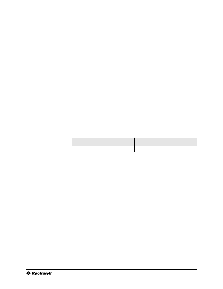
Table 2-6. Crystal Oscillator Circuit Component Values
Component
Value
Y1
32 times the data rate
