12 program operation timing – Samsung MUXONENAND A-DIE KFM2G16Q2A User Manual
Page 155
MuxOneNAND2G(KFM2G16Q2A-DEBx)
- 155 -
FLASH MEMORY
MuxOneNAND4G(KFN4G16Q2A-DEBx)
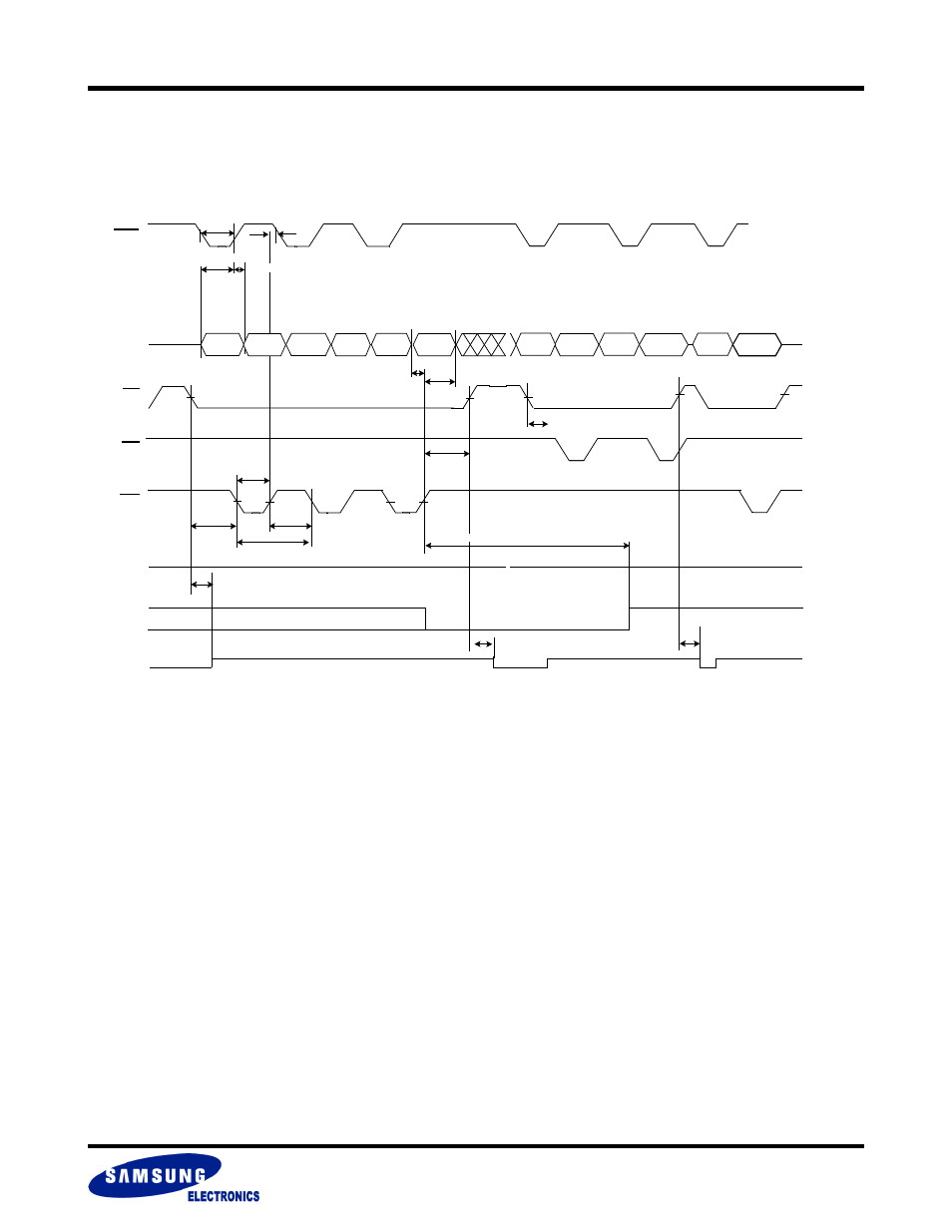
6.12 Program Operation Timing
See AC Characteristics Tables 5.5, 5.7 and 5.9.
NOTE :
1) AA = Address of address register
CA = Address of command register
PCD = Program Command
PMA = Address of memory to be programmed
BA = Address of BufferRAM to write the data
BD = Program Data
SA = Address of status register
AA* = Address of Start Address1 Register(for Flash Block Address)
PMB = DFS & FBA(Flash Block address) of memory to be programmed next time
2) “In progress” and “complete” refer to status register.
3) Status reads in this figure is asynchronous read, but status read in synchronous mode is also supported.
Program Command Sequence (last two cycles)
WE
CE
CLK
t
DS
t
DH
t
CH
t
WPL
t
CS
t
WPH
t
WC
SA
SA
In
Progress
Completed
AA
OE
Read Status Data
V
IL
AVD
BA
CA
PCD
PMA
BD
t
AAVDH
t
AAVDS
INT
t
AVDP
t
WEA
t
CER
A/DQ0:
A/DQ15
RDY
Hi-Z
t
CER
t
CEZ
bit
t
CEZ
≈
≈
≈
≈
≈
≈
t
PGM1 or tPGM2
AA
*
PMB