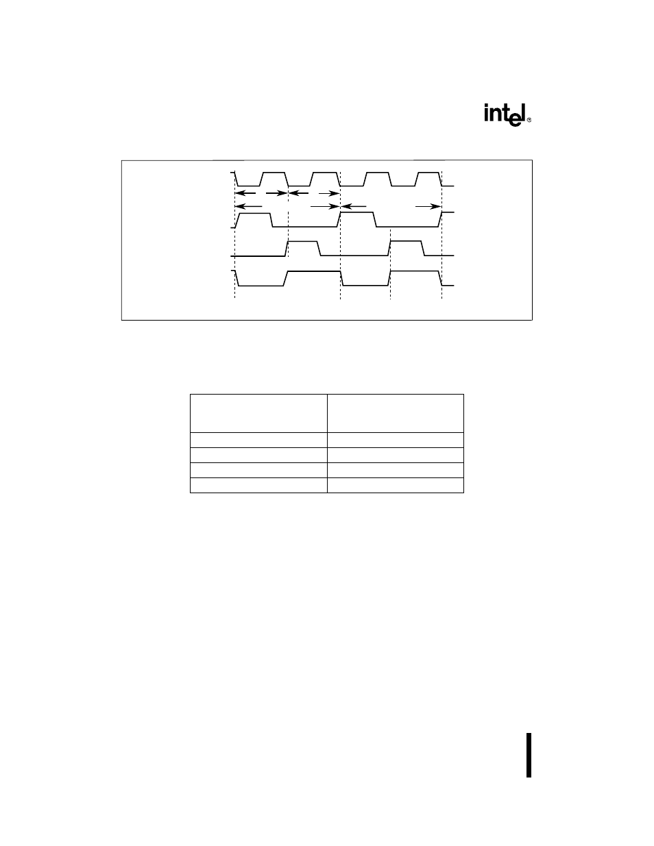
Figure 23. internal clock phases (assumes pll is, Table 22. state times at various frequencies, Internal clock phases (assumes pll is bypassed) -4 – Intel 8XC196Lx User Manual
Page 18: State times at various frequencies -4
8XC196L
X SUPPLEMENT
2-4
Figure 2-3. Internal Clock Phases (Assumes PLL is Bypassed)
The combined period of phase 1 and phase 2 of the internal CLKOUT signal defines the basic
time unit known as a state time or state. Table 2-2 lists state time durations at various frequencies.
The following formulas calculate the frequency of PH1 and PH2, the duration of a state time, and
the duration of a clock period (t).
Because the device can operate at many frequencies, this manual defines time requirements (such
as instruction execution times) in terms of state times rather than specific measurements.
Datasheets list AC characteristics in terms of clock periods (t; sometimes called T
osc
).
Figure 2-4 illustrates the timing relationships between the input frequency (F
XTAL
1
), the operating
frequency (f), and the CLKOUT signal with each PLLEN pin configuration. Table 2-3 details the
relationships between the input frequency (F
XTAL
1
), the PLLEN pin, the operating frequency (f),
the clock period (t), and state times.
Table 2-2. State Times at Various Frequencies
f
(Frequency Input to the
Divide-by-two Circuit)
State Time
8 MHz
250 ns
12 MHz
167 ns
16 MHz
125 ns
20 MHz
100 ns
PH1
PH2
CLKOUT
Phase 1
Phase 2
XTAL1
A0805-01
1 State Time
Phase 1
Phase 2
t
t
1 State Time
PH1 (in MHz)
f
2
---
PH2
=
=
State Time (in µs)
2
f
---
=
t
1
f
---
=