Figure 25. unerasable prom 1 (usfr1) register (la, Table 24. uprom programming values and locations, 5 internal peripherals – Intel 8XC196Lx User Manual
Page 20: Internal peripherals -6, Uprom programming values and locations -6
8XC196L
X SUPPLEMENT
2-6
To program these bits, write the correct value to the locations shown in Table 2-4 using slave pro-
gramming mode. During normal operation, you can determine the values of these bits by reading
the UPROM SFR (Figure 2-5).
You can verify a UPROM bit to make sure it programmed, but you cannot erase it. For this rea-
son, Intel cannot test the bits before shipment. However, Intel does test the features that the UP-
ROM bits enable, so the only undetectable defects are (unlikely) defects within the UPROM cells
themselves.
2.5
INTERNAL PERIPHERALS
The internal peripheral modules provide special functions for a variety of applications. This sec-
tion provides a brief description of the peripherals that differ between the 8XC196Lx and the
8XC196Kx families.
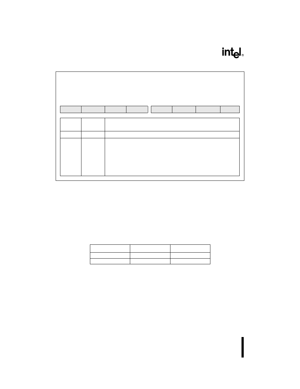
USFR1 (read only)
Address:
Reset State:
1FF2H
XXH
The UPROM special-function register 1 (USFR1) reflects the status of unerasable, programmable
read-only memory (UPROM) locations. This read-only register reflects the status of two bits that
control the output frequency on CLKOUT.
7
0
—
—
—
—
—
—
CLK1
CLK0
Bit
Number
Bit
Mnemonic
Function
7:2
—
Reserved.
1:0
CLK1:0
CLKOUT Control
These bits reflect the programmed frequency of the CLKOUT signal:
CLK1 CLK0
0
0
divide by 1 (CLKOUT = f/2)
0
1
divide by 2 (CLKOUT = f/4)
1
0
divide by 4 (CLKOUT = f/8)
1
1
divide by 1 (CLKOUT = f/2)
Figure 2-5. Unerasable PROM 1 (USFR1) Register (LA, LB Only)
Table 2-4. UPROM Programming Values and Locations
To set this bit
Write this value
To this location
CLK0
0001H
0768H
CLK1
0002H
0728H