Figure 22. clock circuitry (87c196la, lb only), Clock circuitry (87c196la, lb only) -3 – Intel 8XC196Lx User Manual
Page 17
2-3
ARCHITECTURAL OVERVIEW
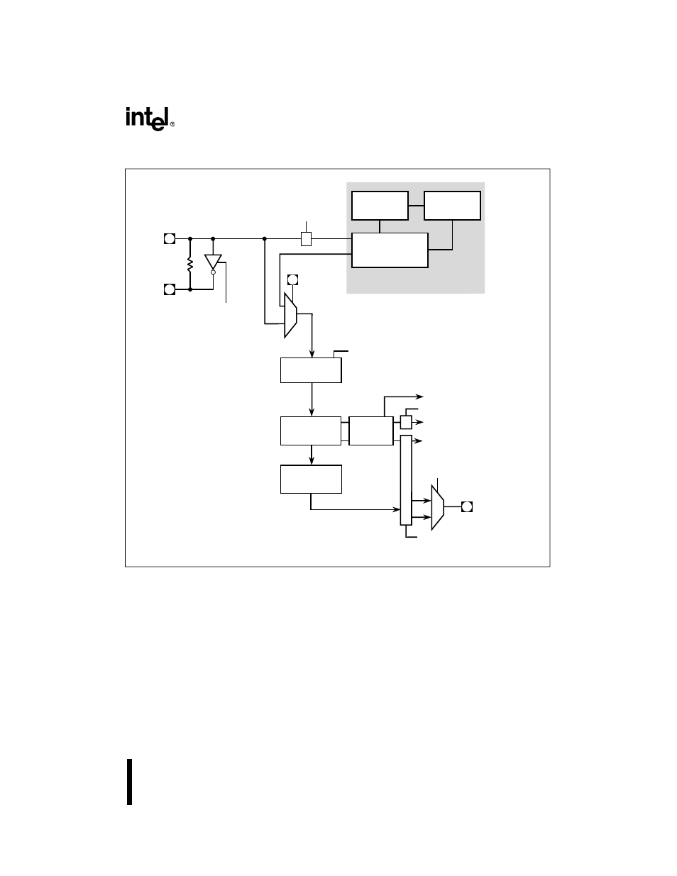
Figure 2-2. Clock Circuitry (87C196LA, LB Only)
The rising edges of PH1 and PH2 generate the internal CLKOUT signal (Figure 2-3). The clock
circuitry routes separate internal clock signals to the CPU and the peripherals to provide flexibil-
ity in power management. It also outputs the CLKOUT signal on the CLKOUT pin. Because of
the complex logic in the clock circuitry, the signal on the CLKOUT pin is a delayed version of
the internal CLKOUT signal. This delay varies with temperature and voltage.
Phase-locked Loop
Clock Multiplier
Phase
Comparator
Filter
Phase-locked
Oscillator
A5290-01
Disable
PLL
(Powerdown)
XTAL1
XTAL2
F
XTAL1
Disable Oscillator
(Powerdown)
0
1
Disable Clocks (Idle, Powerdown)
1
0
PLLEN
2F
XTAL1
Clock
Generators
Programmable
Divider
(CLK1:0)
Disable Clock Input (Powerdown)
CPU Clocks (PH1, PH2)
Peripheral Clocks (PH1, PH2)
Disable Clocks (Powerdown)
CLKOUT
f
f/2
OSC
F
XTAL1
f/2
Divide by two
Circuit
Clock
Failure
Detection
To reset logic