Figure 42. interrupt mask 1 (int_mask1) register, 2 interrupt pending registers, Interrupt pending registers -4 – Intel 8XC196Lx User Manual
Page 38: Interrupt mask 1 (int_mask1) register -4
8XC196L
X SUPPLEMENT
4-4
4.2.2
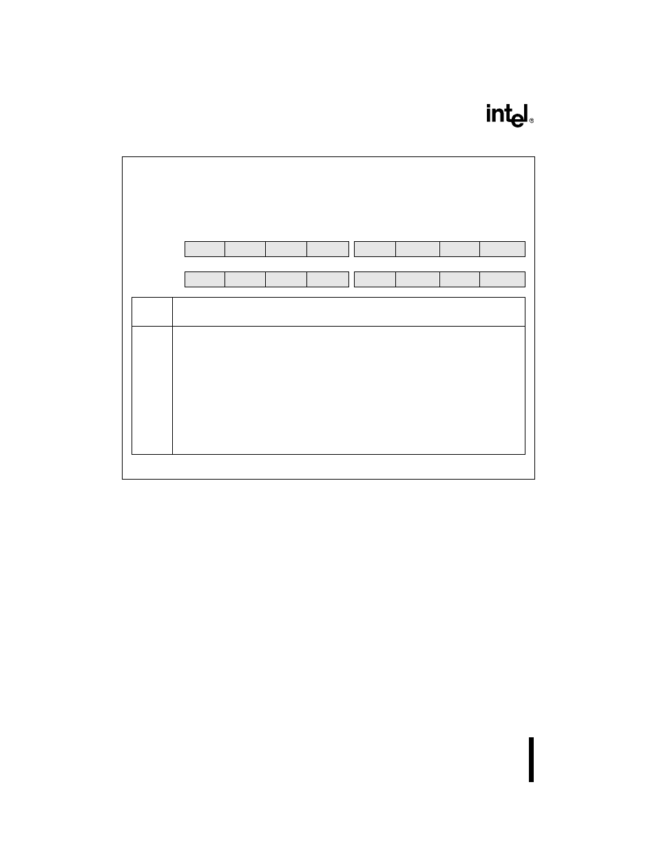
Interrupt Pending Registers
Figures 4-3 and 4-4 illustrate the interrupt pending registers for the 8XC196Lx microcontrollers.
INT_MASK1
Address:
Reset State:
0013H
00H
The interrupt mask 1 (INT_MASK1) register enables or disables (masks) individual interrupt requests.
(The EI and DI instructions enable and disable servicing of all maskable interrupts.) INT_MASK1 can
be read from or written to as a byte register. PUSHA saves this register on the stack and POPA
restores it.
7
0
LB
NMI
EXTINT
—
RI
TI
SSIO1
SSIO0
J1850ST
7
0
LA, LD
NMI
EXTINT
—
RI
TI
SSIO1
SSIO0
—
Bit
Number
Function
7:0
†
Setting a bit enables the corresponding interrupt.
Bit Mnemonic
Interrupt Description
NMI
††
Nonmaskable Interrupt
EXTINT
EXTINT Pin
Reserved
—
RI
SIO Receive
TI
SIO Transmit
SSIO1
SSIO1 Transfer
SSIO0
SSIO0 Transfer
J1850ST
J1850 Status (LB only)
††
NMI is always enabled. This nonfunctional mask bit exists for design symmetry with the
INT_PEND1 register. Always write zero to this bit.
†
Bit 5 is reserved on the 8XC196L
x devices, and bit 0 is reserved on the 87C196LA and 83C196LD.
For compatibility with future devices, always write zeros to these bits.
Figure 4-2. Interrupt Mask 1 (INT_MASK1) Register