Table a3. 83c196ld signals arranged by functional – Intel 8XC196Lx User Manual
Page 114
8XC196L
X SUPPLEMENT
A-6
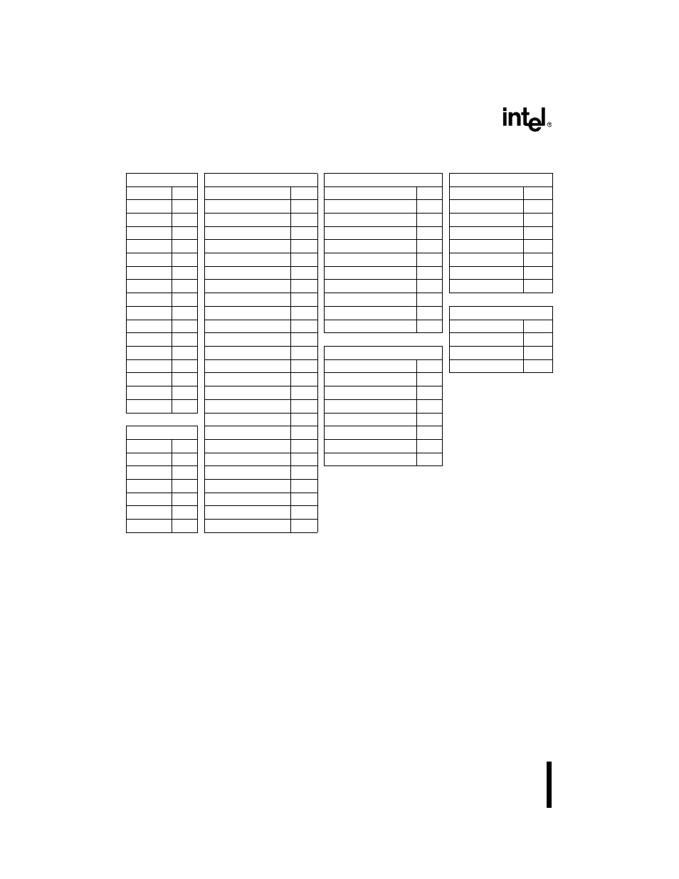
Table A-3. 83C196LD Signals Arranged by Functional Categories
Addr & Data
Input/Output
Input/Output (Cont’d)
Processor Control
Name
Pin
Name
Pin
Name
Pin
Name
Pin
AD0
22
P1.0/EPA0/T2CLK
44
P4.7
7
CLKOUT
32
AD1
21
P1.1/EPA1
43
P5.0
2
EA#
24
AD2
20
P1.2/EPA2/T2DIR
42
P5.2
6
EXTINT
29
AD3
19
P1.3/EPA3
41
P5.3
5
ONCE#
31
AD4
18
P2.0/TXD
27
P6.0/EPA8
45
RESET#
23
AD5
17
P2.1/RXD
28
P6.1/EPA9
46
XTAL1
52
AD6
16
P2.2
29
P6.4/SC0
47
XTAL2
51
AD7
15
P2.4
30
P6.5/SD0
48
AD8
14
P2.6
31
P6.6/SC1
49
Bus Control & Status
AD9
13
P2.7
32
P6.7/SD1
50
Name
Pin
AD10
12
P3.0
22
ADV#/ALE
2
AD11
11
P3.1
21
Power & Ground
RD#
5
AD12
10
P3.2
20
Name
Pin
WR#/WRL#
6
AD13
9
P3.3
19
V
CC
26
AD14
8
P3.4
18
V
CC
40
AD15
7
P3.5
17
V
PP
4
P3.6
16
V
SS
1
Input
P3.7
15
V
SS
3
Name
Pin
P4.0
14
V
SS
25
P0.2
33
P4.1
13
V
SS
39
P0.3
34
P4.2
12
P0.4
35
P4.3
11
P0.5
36
P4.4
10
P0.6
37
P4.5
9
P0.7
38
P4.6
8