Capacitance – Avago Technologies LSI53C120 User Manual
Page 40
3-10
Specifications
provides the minimum and maximum values for these
LSI53C120 SCSI signals.
provides the minimum and maximum values for the
LSI53C120 Input signals.
provides the minimum and maximum values concerning
capacitance for the LSI53C120.
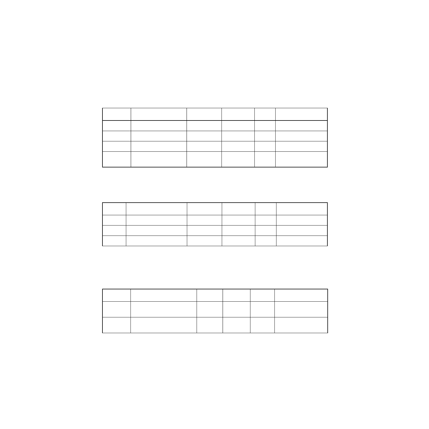
Table 3.11
SCSI Signals – A_SMSG, A_SI_O/, A_SC_D/, A_SATN/, A_SBSY/, A_SSEL/,
A_SRST/, B_SMSG, B_SI_O/, B_SC_D/, B_SATN/, B_SBSY/, B_SSEL/,
B_SRST/
Symbol
Parameter
Min
Max
Unit
Test Conditions
V
IH
Input high voltage
1.9
V
DD
+ 0.5
V
–
V
IL
Input low voltage
V
SS
- 0.5
1.0
V
–
V
OL
Output low voltage
V
SS
0.5
V
48 mA
I
OZ
3-state leakage
(SRST/ only)
-10
-500
10
-50
µ
A
–
Table 3.12
Input Signals – CLOCK, DIFF_SENSE, DIFF_MODE/*, WS_ENABLE/*
Symbol
Parameter
Min
Max
Unit
Test Conditions
V
IH
Input high voltage
2.0
V
DD
+ 0.5
V
–
V
IL
Input low voltage
V
SS
- 0.5
0.8
V
–
I
IN
Input leakage
-10
1
10
µ
A
–
1. The minimum (I
IN
) Input leakage for DIFF_MODE/ and WS_ENABLE/ is -100
µ
A.
Table 3.13
Capacitance
Symbol
Parameter
Min
Max
Unit
Test Conditions
C
I
Input capacitance of input
pads
–
7
pF
–
C
IO
Input capacitance of I/O
pads
–
10
pF
–
- MGA-725M4 (4 pages)
- MGA-71543 (4 pages)
- MGA-71543 (3 pages)
- MGA-82563 (6 pages)
- 3ware SAS 9750-8i (48 pages)
- 3ware 9690SA-8I (Channel) (138 pages)
- 3ware 9690SA-8I (Channel) (380 pages)
- 3ware SAS 9750-8i (29 pages)
- 3ware 9550SXU-8LP (Channel) (149 pages)
- 3ware 9550SXU-8LP (Channel) (40 pages)
- 3ware 9650SE-8LPML (Channel) (45 pages)
- 3ware 9690SA-8I (Channel) (27 pages)
- 3ware 9690SA-8I (Channel) (361 pages)
- 6160 SAS Switch (2 pages)
- MegaRAID SAS 9266-8i (12 pages)
- MegaRAID SAS 9380-8e (43 pages)
- Cache Protection for RAID Controller Cards (139 pages)
- Cache Protection for RAID Controller Cards (13 pages)
- MegaRAID SAS 9271-8iCC (13 pages)
- MegaRAID SAS 9361-8i (13 pages)
- MegaRAID SAS 9266-8i (20 pages)
- MegaRAID SAS 9271-8iCC (26 pages)
- MegaRAID SafeStore Software (502 pages)
- MegaRAID SAS 9285-8ecv (80 pages)
- MegaRAID SAS 9285-8ecv (92 pages)
- MegaRAID SAS 0260CV-4i (64 pages)
- MegaRAID SAS 0260CV-4i (49 pages)
- MegaRAID SAS 9271-8i (8 pages)
- MegaRAID SAS 0260CV-4i (72 pages)
- MegaRAID SAS 9361-8i (7 pages)
- MegaRAID SAS 9341-8i (8 pages)
- MegaRAID SAS 9380-4i4e (7 pages)
- MegaRAID SAS 9380-8e (7 pages)
- MegaRAID SAS 0260CV-4i (28 pages)
- MegaRAID SAS 9240-8i (4 pages)
- MegaRAID SAS 9260-16i (12 pages)
- MegaRAID SAS 9280-24i4e (14 pages)
- MegaRAID SAS 9280-24i4e (16 pages)
- MegaRAID SAS 9260-8i (4 pages)
- MegaRAID SafeStore Software (8 pages)
- MegaRAID SAS 9280-8e (22 pages)
- MegaRAID SAS 9261-8i (4 pages)
- MegaRAID SAS 9285-8e (12 pages)
- MegaRAID SAS 9280-16i4e (12 pages)
- MegaRAID SAS 9280-4i4e (4 pages)