1 data and parity, Data and parity, Lsi53c120 signal grouping – Avago Technologies LSI53C120 User Manual
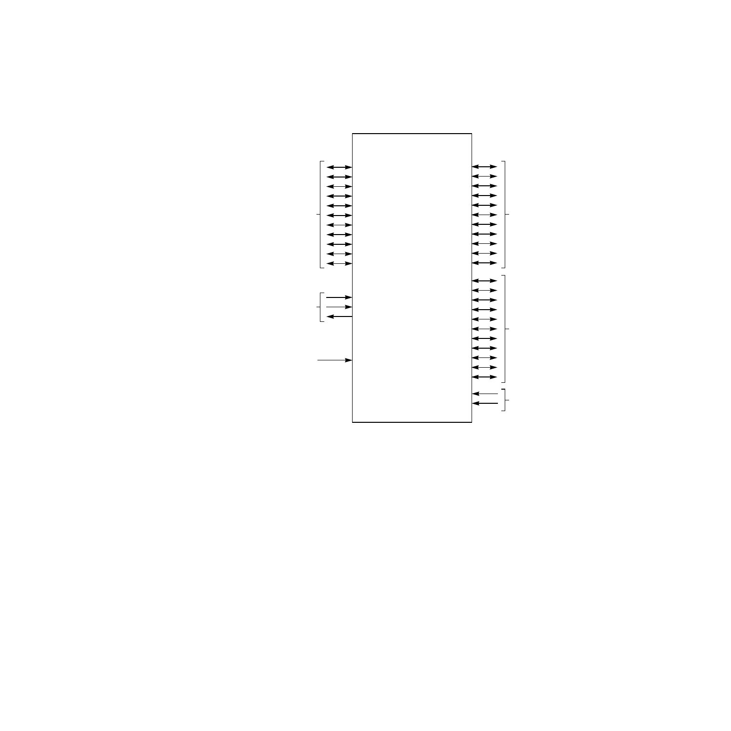
Page 23: Figure 2.2

SCSI Signal Descriptions
2-5
Figure 2.2
LSI53C120 Signal Grouping
2.2.1 Data and Parity
The signals named A_SD[15:0]/ and A_SDP[1:0]/ are the data and parity
signals from the A-side and B_SD[15:0]/ and B_SDP[1:0]/ are the data
and parity signals from the B-side of the LSI53C120. The LSI53C120
sends and receives these signals by using SCSI compatible driver and
receiver logic designed into the LSI53C120 interfaces. This logic
provides the necessary drive, sense thresholds, and input hysteresis to
function correctly in a SCSI bus environment.
The LSI53C120 receives data and parity signals and passes them from
the source bus to the load bus and provides any necessary edge shifting
to guarantee the skew budget for the load bus. Either side of the
SCSI A
Data and Control
SCSI B
Differential
Control
LSI53C120
CLOCK
Clock Input
Control Signals
SCSI B
Data and
Control
Transceiver
Control
A_SD[15:0]/
A_SDP[1:0]/
A_SC_D/
A_SI_O/
A_SMSG/
A_SREQ/
A_SACK/
A_SBSY/
A_SATN/
A_SSEL/
A_SRST/
B_SD15:0]/
B_SDP[1:0]/
B_SC_D/
B_SI_O/
B_SMSG/
B_SREQ/
B_SACK/
B_SBSY/
B_SATN/
B_SSEL/
B_SRST/
RESET/
WS_ENABLE/
XFER_ACTIVE
B_SD[15:-0]/
B_SDP[1:0]/
B_SC_D/
B_SI_O/
B_SMSG/
B_SREQ/
B_SACK/
B_SBSY/
B_SATN/
B_SSEL/
B_SRST/
DIFF_SENSE
DIFF_MODE/
