Scsi a-side and b-side single-ended control blocks, Lsi53c120 block diagram, Figure 2.1 – Avago Technologies LSI53C120 User Manual
Page 20
2-2
Functional Description
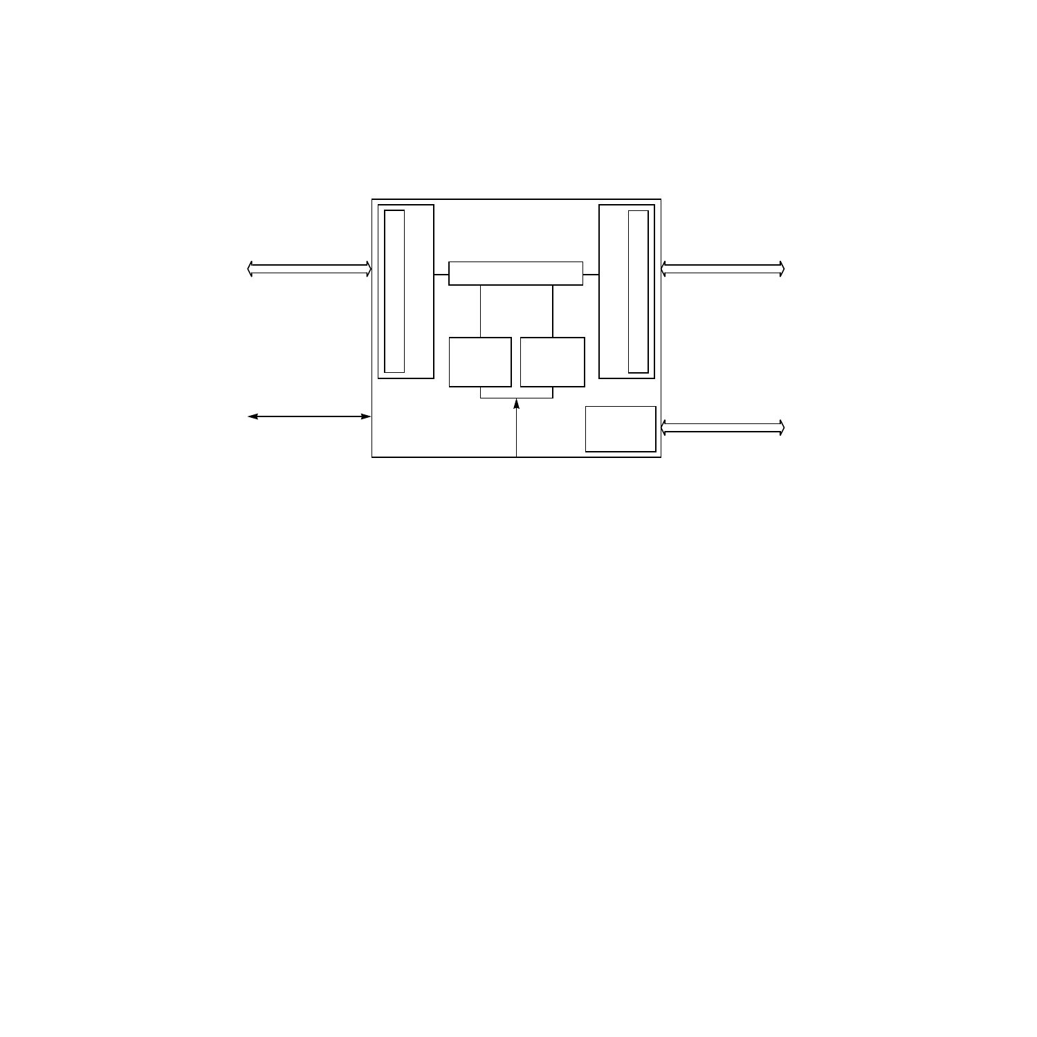
Figure 2.1
LSI53C120 Block Diagram
In its simplest form, the LSI53C120 passes data and parity from a source
bus to a load bus. The side asserting, deasserting or releasing the SCSI
signals is the source side. The model of the LSI53C120 represents
pieces of wire that allow corresponding SCSI signals to flow from one
side to the other side. The LSI53C120 monitors arbitration and selection
by devices on the bus so it can enable the proper drivers to pass the
signals along. In addition, the LSI53C120 does some signal re-timing to
maintain the signal skew budget from source bus to load bus.
2.1.1 SCSI A-Side and B-Side Single-Ended Control Blocks
In the Single-ended (SE) to Single-ended mode, the SCSI A-side pins
are connected internally to the corresponding SCSI B-side pins, forming
bi-directional connections to the SCSI bus.
The SCSI A-side and B-side SE control blocks connect to both targets
and initiators and accept any asynchronous or synchronous data transfer
rates up to the 40 Mbytes/s rate of Wide Ultra SCSI. TolerANT
technology is part of the SCSI A-side and B-side SE control blocks.
Single-ended
Wide Ultra SCSI Bus
A-Side
Single-ended
Wide Ultra SCSI Bus
B-Side
40 Mhz Clock Input
Control Signals
Control
Control
Chip Boundary
Re-timing Circuit
Precision
Delay
Control
State
Machine
Control
T
olerANT Dr
iv
ers and Receiv
ers
SCSI Control Bloc
k
Differential
Control
Data and Control
Data and Control
Wide Ultra SCSI Bus
High Voltage Differential
Transceiver Control
or
T
olerANT Dr
iv
ers and Receiv
ers
SCSI Control Bloc
k