Measurement Computing Daq PC-Card User Manual
Page 49
Daq* Hardware
DaqBoards [ISA-types Only]
DaqBook / DaqBoard [ISA-types] / Daq PC-Card User’s Manual
10-18-00
Daq* Hardware 3-19
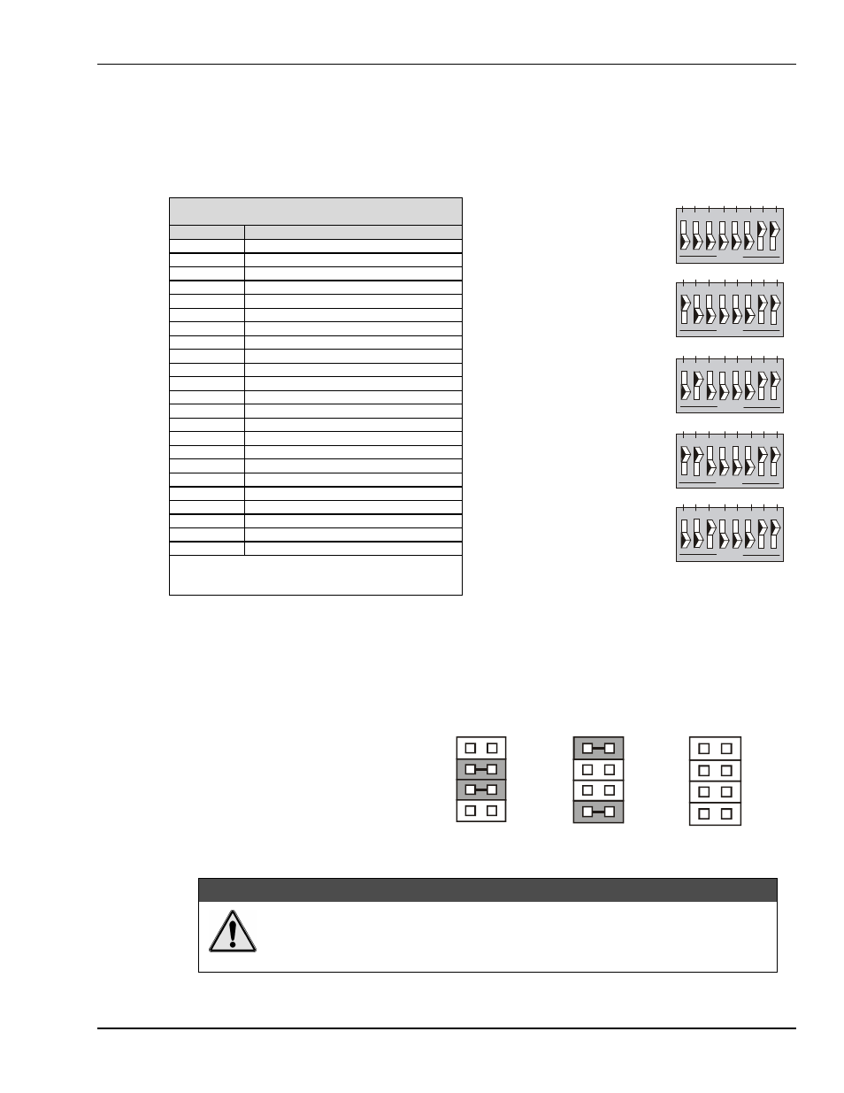
Base Address (SW1)
The computer must know the DaqBoard’s base address. Check the base address setting (3-digit hex) on the
Base Address switch (see figure). The factory default is 300 hex (within the standard range for a prototype
card; see table). If the default value does not work, you must select an address within 200 to 3FF (256 to
1023 decimal). In addition, the address must be on a 4-byte boundary, and it must not conflict with
addresses already in use.
External Analog Expansion Power (JP1)
This 4×2 header (JP1) has 3 possible
settings. If analog option cards (DBKs) are
used, the JP1 pins are set to provide
±15 VDC to the cards. If such cards are
not used, the counter/timer CTR0 is
available, and JP1 must be set accordingly.
The default setting is for use of analog
option cards.
&$87,21
If using a DBK32A Auxiliary Power Supply or a DBK33 Triple-Output Power
Supply Card, the JP1 shunt jumpers must be entirely removed. Placing the
jumpers on -OCTOUT and -OCLKIN will damage the 8254 timer chip.
Refer to the
Power Management
section in chapter 7, DBK Option Cards and Modules, as needed.
Industry Standard I/O Addresses
Note: Systems vary. This is only a guide.
Hex Range
Device
000-1FF
Internal system
200-207
Game I/O
20C-20D
Reserved
21F
Reserved
278-27F
Parallel printer port 2
2B0-2DF
Alternate enhanced graphics adapter
2E1
GPIB (Adapter 0)
2E2 & 2E3
Data acquisition (Adapter 0)
2F8-2FF
Serial port 2
300-31F
Prototype card
360-363
PC network (low address)
364-367
Reserved
368-36B
PC network (high address)
36C-36F
Reserved
378-37F
Parallel printer port 1
380-38F
SDLC, bisynchronous 2
390-393
Reserved
3A0-3AF
Bisynchronous 1
3B0-3BF
Monochrome display and printer adapter
3C0-3CF
Enhanced graphics adapter
3D0-3DF
Color/Graphics monitor adapter
3F0-3F7
Diskette Controller
3F8-3FF
Serial port 1
Note: I/O addresses, hex 000 to 0FF, are reserved for
the system board I/O. Hex 100 to 3FF are available on
the I/O channel.
304
308
30C
310
300
Fa ctory
D e fau lt
0
1
6 7 8
5
2 3
1
4
O P E N
A2 A3 A4 A5 A6 A7 A8 A9
0
1
6 7 8
5
2 3
1
4
O P E N
A2 A3 A4 A5 A6 A7 A8 A9
0
1
6 7 8
5
2 3
1
4
O P E N
A2 A3 A4 A5 A6 A7 A8 A9
0
1
6 7 8
5
2 3
1
4
O P E N
A2 A3 A4 A5 A6 A7 A8 A9
0
1
6 7 8
5
2 3
1
4
O P E N
A2 A3 A4 A5 A6 A7 A8 A9
Sample Base Addresses on SW1
JP 1
-1 5 V
-O C TO U T
-O C L K IN
+1 5 V
A n a lo g O ptio n
C ard U se
JP 1
-1 5V
-O C TO U T
-O C L K IN
+1 5 V
C o un te r/Tim e r U se
(1 6-bit m o d e on ly)
JP 1
-1 5 V
-O C TO U T
-O C L K IN
+1 5 V
D B K 3 2A o r D B K 3 3
O p tio n C a rd U se
JP1 External Analog Expansion Settings