Switches and jumpers – Measurement Computing Daq PC-Card User Manual
Page 48
DaqBoards [ISA-Types Only]
Daq* Hardware
3-18 Daq* Hardware
10-18-00
DaqBook / DaqBoard [ISA-types] / Daq PC-Card User’s Manual
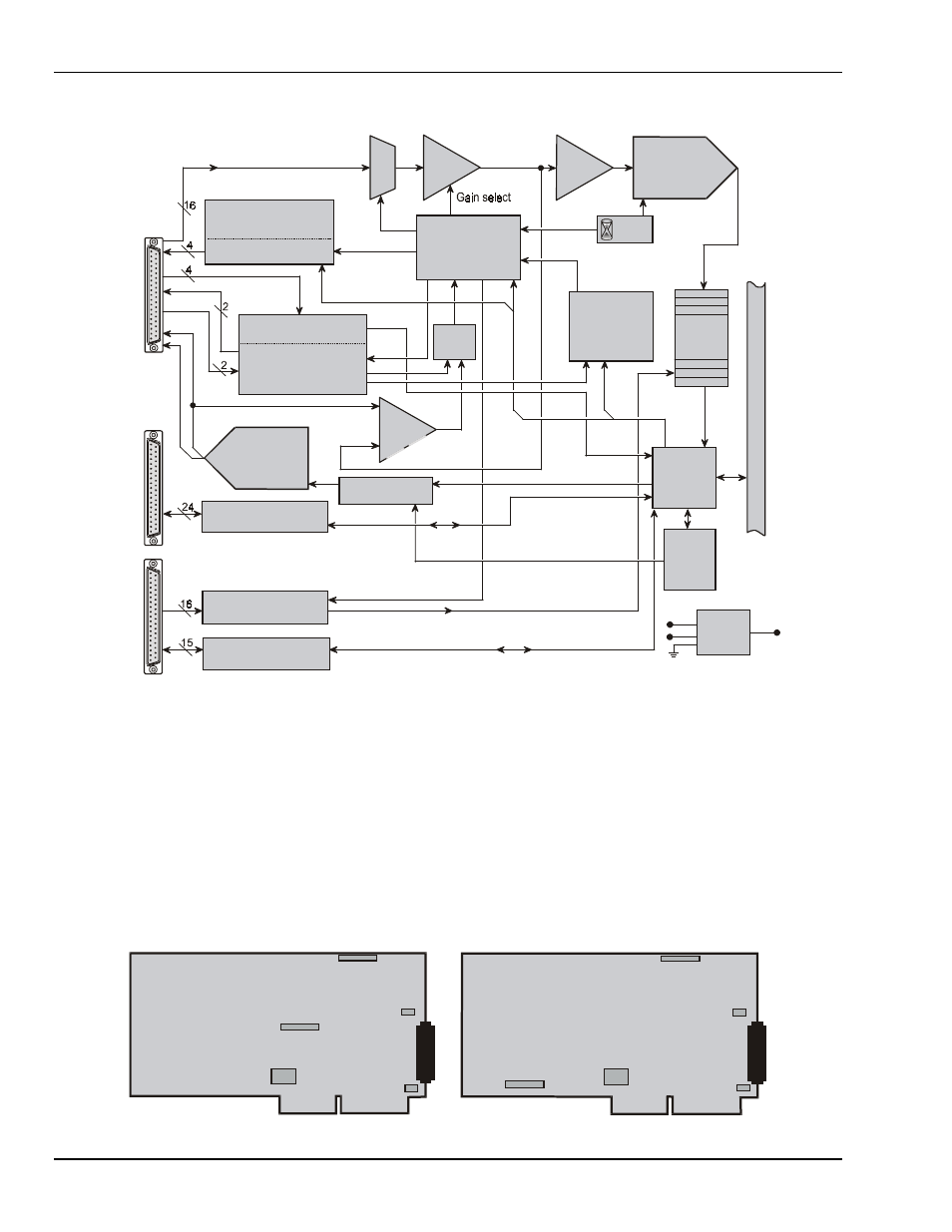
This figure shows a block diagram of DaqBoard models /100A, /112A, /200A, and /216A.
8 D E /16 S E
ana log inpu t
m ultiplex er
512-s tep
random acc ess
channel/gain
sequencer
Trigger
S elec t
P C (IS A )
B us
Interface
16-bit data
& add res s bus
D M A &
Interru pt
Interface
P rog ra m m a ble
s eq ue nc er
tim eb as e.
10 u s to 12 hrs
24-bit gen era l pu rp ose
digita l I/O lines
A n optional adap ter ca ble (C A -6 0) is
require d for ex ternal ac cess to 40-pin
ports P 2 and P 3 (loc ated on D aq B oa rds ).
16 h igh -s peed
digita l inputs
*M odels /1 00A and /2 00A .
5 c ounter/tim e r
c hanne ls
-or-
4 digital outputs
for high-speed
channel ex pans ion
4 general purpose
digital outputs
4K w ord
F IFO
data
buffer
S ignal
I/O
S eq ue nc er
res e t
B lo c k D ia g ra m fo r D a q B o a rd M od e ls /10 0 A , /11 2 A . /20 0 A , /2 1 6A
P 1
A N A LO G I/O
(D A S -1 6
c om pa tible)
P 2 *
D IG ITA L I/O
(P IO -12
c om pa tible)
P 3 *
P U LS E /F R E Q .
H IG H -S P E E D
D IG ITA L I/O
(C T M -05
c om pa tible)
P G A
per c han nel
c ontrol
E x terna l
M U X
A m plifier
S a m ple
&
H old
x 1, x 2
x 4, x 8
100 k H z
C lo ck
4 ge neral purpos e
digita l inputs
-or-
1 a uxiliary c ou nter gate
1 T T L trigger input
2 g ain selec t outputs for
ex pan sion bo ards
D C -D C
c onv erter
P C + 5V
P o w er S upp ly
+ 15
-15
A n alo g Trigge r-In
C om parator
12 or 16-bit,
100 kH z
analog-to-digital
conv erter
A D C
D ual 12-bit
digita l-to-
ana log
c onv erter
D ual-D A C
P
C
(I
S
A
)
B
u
s
4K - w ord F IF O
D ata B uffer
}
Switches and Jumpers
The configuration of all 4 DaqBoard models is similar except for jumper locations. (Refer to the diagram
that matches your model.) The internal configuration of each DaqBoard model consists of setting the
following switches and jumpers for the desired mode of operation:
•
SW1 - Base Address
•
JP1 - External Analog Expansion Power
•
JP2 - DAC Voltage Reference Header
•
JP7 - Calibration (refer to
Calibration
).
•
JP8 - Interrupt & DMA
JP 8
S W 1
S W 1
JP 7
JP 7
JP 8
JP 2
JP 2
JP 1
JP 1
0
1
0
1
Base Address
Base Address
D a qB o ard/1 00 A /112 A M othe rbo a rd
D a qB o ard/2 00 A /21 6A M o th erb oa rd
Location of DaqBoard Jumpers