Chapter 3 bios description – Foxconn 865A01-PE-6EKRS User Manual
Page 59
51
Chapter 3 BIOS Description
865A01 G/PE User Manual
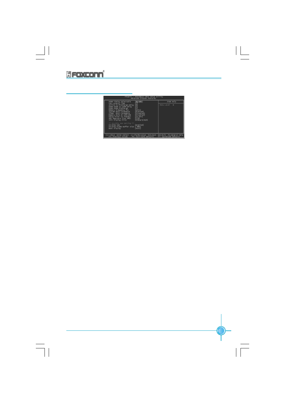
Advanced Chipset Features
DRAM Timing Selectable (Default: By SPD)
This option is used to set the signal time sequence of the DRAM. The “By
SPD” DRAM speed is controlled by the DRAM data register, and the “By
Manual” DRAM speed is controlled by the user.
CAS Latency Time (Default: depend on memory)
This item determines CAS Latency. The available setting values are: 2,
2.5 and 3.
Active to Precharge Delay (Default: depend on memory)
This item allows you to select DRAM Active to Precharge Delay. The
available setting values are: 8, 7, 6 and 5.
DRAM RAS# to CAS# Delay (Default: depend on memory)
This item allows you to select a delay time between the CAS and RAS
strobe signals. The available setting values are: 4, 3, and 2.
DRAM RAS# Precharge (Default: depend on memory)
This item allows you to select the DRAM RAS# precharge time. The
available setting values are: 4, 3, and 2.
Memory Frequency For (Default: Auto)
It sets the frequency for memory.
Note: The operating frequency will be 320MHz when a 800MHz CPU and
a DDR333MHz are used jointly.
System BIOS Cacheable (Default: Enabled)
This option is used to determine whether the system BIOS is written into
the buffer memory. The available setting values are: Disabled and Enabled.
Advanced Chipset Features Setup
865A01-FOXCONN-V1.3-EN-121603.p65
2004-5-27, 18:02
51