B.5 card clock architecture, Figure b-6, Card clock scheme – Artesyn PCIE-8120 Installation and Use (July 2014) User Manual
Page 61: Card clock architecture, Pcie-8120 hardware description, Dc/dc disable for vp12 < 8.5v (calculated)
PCIE-8120 Hardware Description
PCIE-8120 Installation and Use (6806800R89C)
61
According to the PCI Express Card Electromechanical Specification Rev.2.0.2007.PCISIG CEM
2.04/11/2007, the PERST# signal indicates a system power good status combined with a card
reset function. Therefore, it cannot be used as a power good signal to the cards power-up
control for the local DC/DC units. To keep up with the timing requirements for the PERST#
signal, the local power control must enable the DC/DC units immediately after card edge
power appears. An undervoltage-lockout circuitry is used to provide a status signal that
indicates when the 12V main supply is within the allowed range:
DC/DC enable for VP12 > 11.08V (calculated)
DC/DC disable for VP12 < 8.5V (calculated)
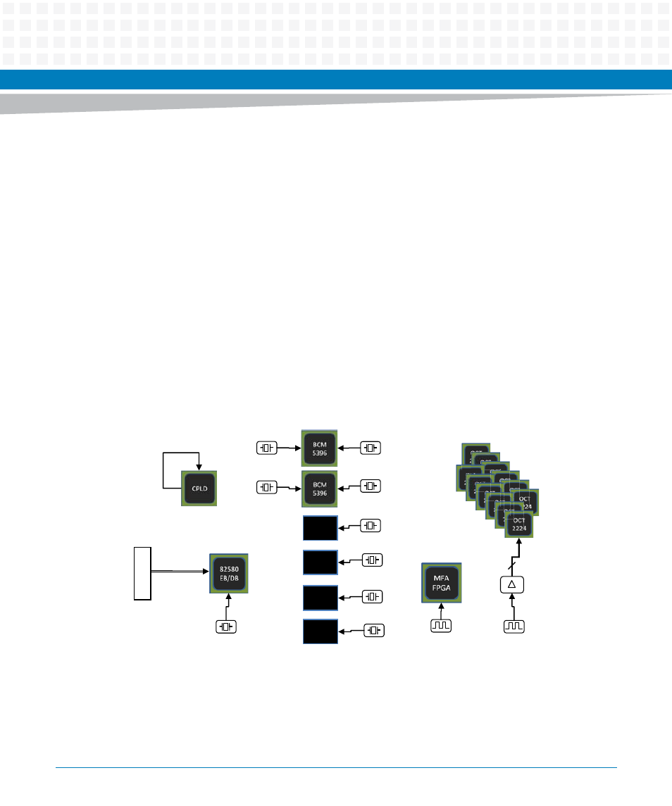
B.5
Card Clock Architecture
The following figure provides an overview of the Card Clock Architecture of PCIE-8120:
Figure B-6
Card Clock Scheme
PCIe_
x4
25.000MHz
PCIe_ RefCLK
100MHz
25.000MHz
20MHz
PHY
88E1512
PHY
88E1111
PHY
88E1512
PHY
88E1111
25.000MHz
25.000MHz
25.000MHz
25.000MHz
25.000MHz
25.000MHz
25.000MHz
25.000MHz
25.000MHz
LVC x12 buffer
12
- ARTM-9405 16x10GbE Installation and Use Guide (May 2014) (64 pages)
- ATCA 7370 / ATCA 7370-S Installation and Use (January 2015) (256 pages)
- ATCA 7370 / ATCA 7370-S Installation and Use (September 2014) (254 pages)
- ARTM-831X Installation and Use (June 2014) (346 pages)
- ATCA-7350 - Integrating with Workbench User Guide (September 2014) (34 pages)
- ATCA-7350 Installation and Use (September 2014) (208 pages)
- ATCA-7365-CE Installation and Use (Jan 2015) (300 pages)
- ATCA-7365-CE Installation and Use (May 2014) (294 pages)
- ATCA-7365-CE Installation and Use (May 2014) (306 pages)
- ATCA-7368 Installation and Use (June 2014) (222 pages)
- ATCA-7475 Installation and Use (October 2014) (284 pages)
- ATCA-7480 Installation and Use (April 2015) (330 pages)
- ATCA-8330 Installation and Use (April 2015) (236 pages)
- ATCA-8320 Installation and Use (May 2014) (456 pages)
- ATCA-9305 User's Manual (May 2014) (270 pages)
- ATCA-9405 Installation and Use (October 2014) (168 pages)
- ATCA-F120 Installation and Use (August 2014) (122 pages)
- ATCA-F140 Installation and Use (September 2014) (138 pages)
- ATCA-MF106 Installation and Use (September 2014) (86 pages)
- Centellis-4440/AXP1440 Installation and Use (September 2014) (208 pages)
- Centellis 4410 (AXP-1410) Installation and Use (July 2014) (202 pages)
- Centellis 2100 Release 3.0 Installation and Use (March 2015) (192 pages)
- Centellis 2100 Release 3.0 Installation and Use (March 2015) (176 pages)
- Centellis 2000 User Card-10GE Installation and Use (May 2014) (54 pages)
- Centellis 2000 User Card-10GE with Telco Alarm Installation and Use (May 2014) (60 pages)
- COMX-CAR-210 Installation and Use (August 2014) (76 pages)
- COMX-P1022 Installation and Use (July 2014) (84 pages)
- COMX-P2020 Installation and Use (February 2015) (100 pages)
- COMX-CORE Series Installation and Use (August 2014) (128 pages)
- COMX-P2020 Installation and Use (July 2014) (100 pages)
- COMX-P4080-2G-ENP2 Installation and Use (August 2014) (70 pages)
- COMX-P4080 Installation and Use (August 2014) (126 pages)
- COMX-P40x0 ENP2 Installation and Use (August 2014) (130 pages)
- COMX-P40x0 ENP2 Installation and Use (January 2015) (140 pages)
- iVPX7225 RTM Installation and Use (April 2015) (56 pages)
- MITX-430/MITX-440-DVI-2E Installation and Use (August 2014) (118 pages)
- CPCI-6200 Installation and Use (May 2015) (234 pages)
- SCP-MITX-CORE-820-SM Installation and Use (August 2014) (132 pages)
- iVPX7225 Installation and Use (April 2015) (168 pages)
- MVME2502 Installation and Use (August 2014) (150 pages)
- MVME2502 Installation and Use (December 2014) (166 pages)
- MVME2500 VxWorks 6.8 AMP User Guide (August 2014) (40 pages)
- MVME2500 VxWorks 6.8 User Guide (April 2014) (44 pages)
- MVME3100 Single Board Computer Installation and Use (June 2014) (156 pages)
- MVME4100 Single Board Computer Installation and Use (June 2014) (136 pages)