Altera Cyclone III LS FPGA Development Board User Manual
Page 54
2–46
Chapter 2: Board Components
Power Supply
Cyclone III LS FPGA Development Board Reference Manual
© October 2009 Altera
Corporation
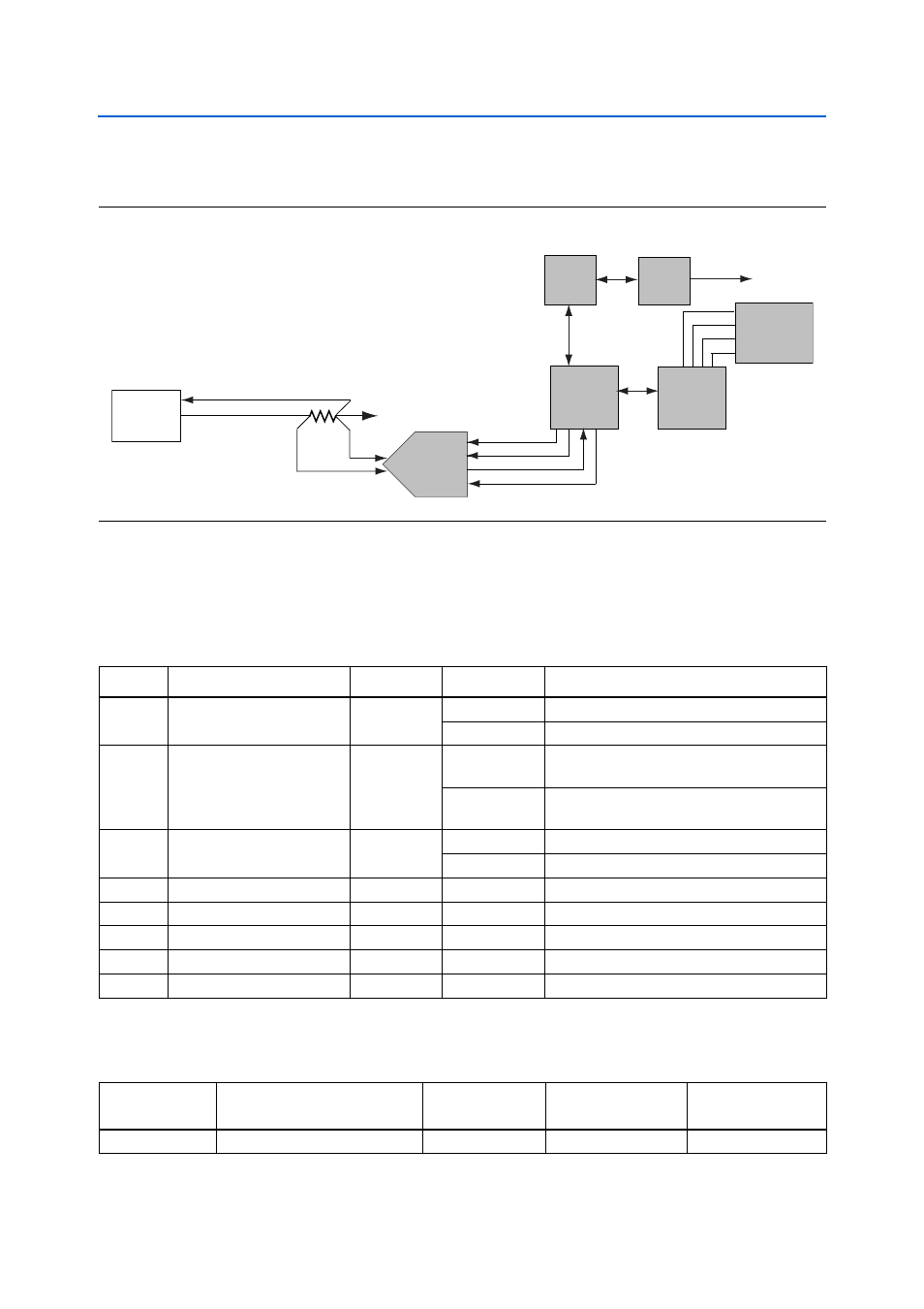
shows the block diagram for the power measurement circuitry.
lists the targeted rails. The schematic signal name column specifies the
name of the rail being measured and the device pin column specifies the devices
attached to the rail. If no subnet is named, the power is the total output power for that
voltage.
lists the power measurement ADC component reference and
manufacturing information.
Figure 2–11. Power Measurement Circuit
SCK
DSI
DSO
CSn
8 Ch.
Power Supply Load # 0-7
Supply
0-7
R
SENSE
3 m
Ω
EPM2210
3CLS200
EPM
240
Z
USB
PHY
To User PC
Power GUI
JTAG Chain
Embedded
USB-Blaster
Feedback
14-pin
2x16 LCD
E
RW
RS
D(0:7)
Table 2–46. Power Rails Measurement Based on the Rail Selected in the Power GUI
Switch
Schematic Signal Name
Voltage (V)
Device Pin
Description
1
VCCIO_B1B2
2.5
VCCIO1
FPGA I/O power bank 1 (HSMB)
VCCIO2
FPGA I/O power bank 2 (HSMB, flash)
2
VCCIO_B3B4
2.5
VCCIO3
FPGA I/O power bank 3 (MAX II, SSRAM,
flash, FSM, Ethernet, user I/O)
VCCIO4
FPGA I/O power bank 4 (MAX II, SSRAM,
flash, FSM, Ethernet)
3
VCCIO_B5B6
2.5
VCCIO5
FPGA I/O power bank 5 (HSMA)
VCCIO6
FPGA I/O power bank 6 (HSMA)
4
VCCIO_B7
1.8
VCCIO7
FPGA I/O power bank 7 (DDR2, user I/O)
5
VCCIO_B8
1.8
VCCIO8
FPGA I/O power bank 8 (DDR2, user I/O)
6
C3LS_VCCINT
1.2
VCCINT
FPGA core power
7
VCCD_PLL
1.2
VCCD_PLL
FPGA PLL digital power
8
C3LS_VCCA
2.5
VCCA
FPGA PLL analog power
Table 2–47. Power Measurement ADC Component Reference and Manufacturing Information
Board Reference
Description
Manufacturer
Manufacturing
Part Number
Manufacturer
Website
U1
8-channel differential 24-bit ADC
Linear Technology
LTC2418CGN#PBF