Jtag chain header switch –18, Table 2–11, Shows – Altera Cyclone III LS FPGA Development Board User Manual
Page 26
2–18
Chapter 2: Board Components
Configuration, Status, and Setup Elements
Cyclone III LS FPGA Development Board Reference Manual
© October 2009 Altera
Corporation
lists the board settings DIP switch component reference and
manufacturing information.
JTAG Chain Header Switch
The JTAG chain header switch (J11) is provided to either remove or include devices in
the active JTAG chain. However, the Cyclone III LS FPGA device is always in the
JTAG chain. Refer to
for the JTAG chain functionality.
shows the switch controls and its descriptions.
Table 2–11. Board Settings DIP Switch Controls
Switch Schematic Signal Name
Description
Default
1
MAX_DIP0
Reserved
ON
2
MAX_DIP1
Reserved
ON
3
AT_ACTIVE
ON: Anti-Tamper example design disable
OFF: Anti-Tamper example design enable
ON
4
JTAG_SECURE
ON: Cyclone III LS JTAG lock feature inactive
OFF: Cyclone III LS JTAG lock feature active
ON
5
USB_DISABLEn
ON : Embedded USB-Blaster disable
OFF : Embedded USB-Blaster enable
OFF
6
USER_PGM
ON: Load factory design from flash memory upon power-up
OFF: Load user hardware page 1 from flash memory upon power-up
ON
7
CLK_ENABLE
ON : On-board oscillators enable
OFF : On-board oscillators disable
OFF
8
CLK_SEL
ON : Programmable oscillator clock select
OFF : SMA input clock select
OFF
Note to
:
(1) ON indicates a setting of ’0’ while OFF indicates a setting of ’1’.
Table 2–12. Board Settings DIP Switch Component Reference and Manufacturing Information
Board Reference
Description
Manufacturer
Manufacturer
Part Number
Manufacturer Website
SW2
Eight-position rocker DIP switch
Grayhill
76SB08ST
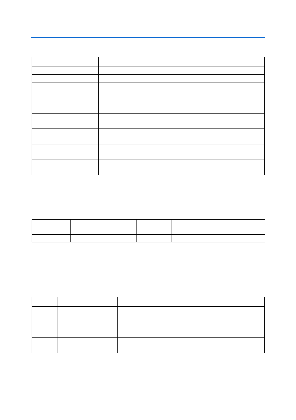
Table 2–13. JTAG Chain Header (J11) Switch Controls
Switch
Schematic Signal Name
Description
Default
1
EPM2210_JTAG_EN
ON : MAX II CPLD EPM2210 System Controller in-chain
OFF : Bypass MAX II CPLD EPM2210 System Controller
ON
2
HSMA_JTAG_EN
ON : HSMA in-chain
OFF : Bypass HSMA
OFF
3
HSMB_JTAG_EN
ON : HSMB in-chain
OFF : Bypass HSMB
OFF