Memory, Memory –35 – Altera Cyclone III LS FPGA Development Board User Manual
Page 43
Chapter 2: Board Components
2–35
Memory
© October 2009 Altera Corporation
Cyclone III LS FPGA Development Board Reference Manual
lists the HSMC connector component reference and manufacturing
information.
Memory
This section describes the board's memory interface support and also their signal
names, types, and connectivity relative to the Cyclone III LS device. The board has the
following memory interfaces:
■
DDR2
■
SSRAM
■
Flash
■
EEPROM
f
For more information about the memory interfaces, refer to the following documents:
■
■
U27.7
Dedicated CMOS I/O bit 73 when
LCD_HSMB_SEL is set to a logic 1.
LCD_HSMB_D73
2.5-V
W4
U27.12
Dedicated CMOS I/O bit 74 when
LCD_HSMB_SEL is set to a logic 1.
LCD_HSMB_D74
W6
U27.9
Dedicated CMOS I/O bit 75 when
LCD_HSMB_SEL is set to a logic 1.
LCD_HSMB_D75
W7
J1.155
LVDS or CMOS clock out 2 or CMOS bit 76
HSMB_CLKOUT_P2
T6
J1.156
LVDS or CMOS clock in 2 or CMOS bit 77
HSMB_CLKIN_P2
T2
J1.157
LVDS or CMOS clock out 2 or CMOS bit 77
HSMB_CLKOUT_N2
T5
J1.158
LVDS or CMOS clock in 2n or CMOS bit 79
HSMB_CLKIN_N2
T1
J1.160
HSMC port B presence detect LED
HSMB_PRSNTn
—
J18
To control the HSMB_D[65:75] via the FPGA,
the shunt should be removed from this jumper,
or the FPGA must drive a logic 1.
LCD_HSMB_SEL
1.8-V
D20
Note to
:
(1) Board references J1.1 to J1.32 are not connected.
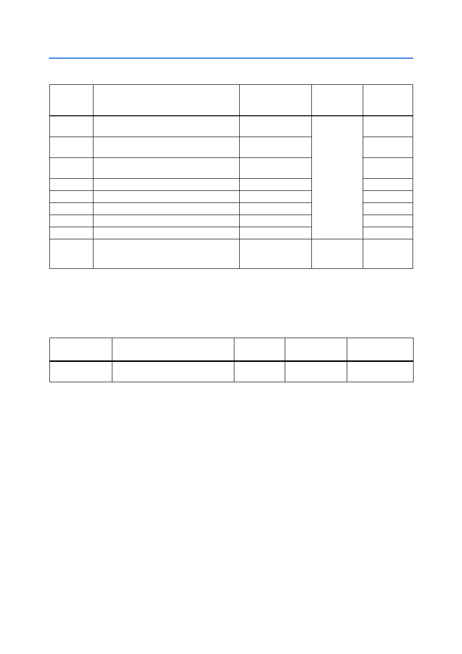
Table 2–35. HSMC Port B Pin Assignments, Schematic Signal Names, and Functions (Part 4 of 4)
(1)
Board
Reference
Description
Schematic Signal
Name
I/O Standard
Cyclone III LS
Device
Pin Number
Table 2–36. HSMC Connector Component Reference and Manufacturing Information
Board Reference
Description
Manufacturer
Manufacturing
Part Number
Manufacturer
Website
J1 and J2
HSMC, custom version of QSH-DP
family high-speed socket.
Samtec
ASP-122953-01