Altera Cyclone III LS FPGA Development Board User Manual
Page 11
Chapter 2: Board Components
2–3
Board Overview
© October 2009 Altera Corporation
Cyclone III LS FPGA Development Board Reference Manual
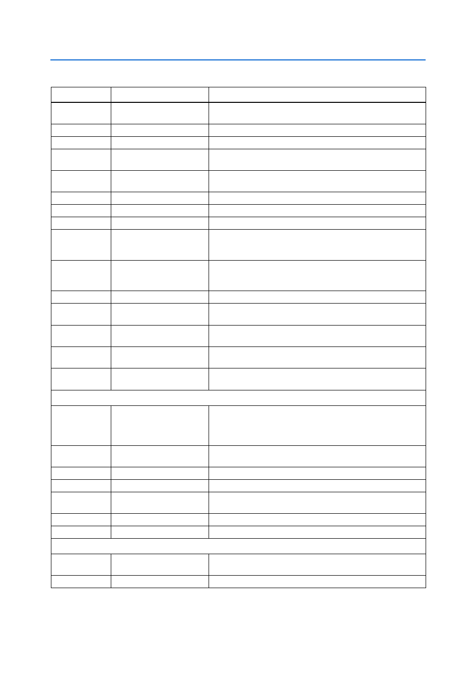
D11
Load LED
Illuminates when the MAX II CPLD EPM2210 System Controller is
actively configuring the FPGA.
D10
Error LED
Illuminates when the FPGA configuration from flash memory fails.
D12
Factory LED
Illuminates when the factory image is loaded to the FPGA.
D29, D30, D31
Configuration select LEDs
Illuminates to show the LED sequence that determines which flash
memory image loads to the FPGA when PGM SEL is pressed.
D15, D16, D18,
D20, D22
Ethernet LEDs
Shows the connection speed as well as transmit or receive activity.
D2
HSMC port A present LED
Illuminates when a daughtercard is plugged into the HSMC port A.
D1
HSMC port B present LED
Illuminates when a daughtercard is plugged into the HSMC port B.
D3
Power LED
Illuminates when 12-V power is present.
J18
LCD/HSMC Port B data select
Controls data multiplexing to the FPGA from the LCD or
HSMB_D[65:75]. Placing a shunt on the jumper allows the FPGA to
control the LCD signals.
J6
PS standard/fast select
Placing a shunt sets the MSEL pins for passive serial standard
configuration. Otherwise, the MSEL pins is set for passive serial fast
configuration.
S2
CPU reset push-button switch
Press to reset the FPGA logic.
S11
VCCA shutdown push-button
switch
Turns VCCA power to the FPGA on and off. This switch initiates a
power-on reset.
S10
MAX II reset push-button
switch
Press to reset the MAX II CPLD EPM2210 System Controller.
S9
PGM select push-button
switch
Toggles the PGM LEDs which selects the program image that loads
from flash memory to the FPGA.
S8
PGM configure push-button
switch
Configure the FGPA from flash memory based on the PGM LEDs
setting.
Clock Circuitry
U17
Programmable oscillator
(125 MHz default)
Programmable oscillator with a default frequency of 125.00 MHz. The
frequency is programmable using the MAX II CPLD EPM2210 System
Controller. For general use such as HSMC logic or gigabit Ethernet
(125 M/156.25 M)
X3
66.6 MHz oscillator
66.6 MHz crystal oscillator for general purpose logic and DDR2
memory.
X5
50 MHz oscillator
50 MHz crystal oscillator for general purpose logic.
Y3
100 MHz oscillator
100 MHz crystal oscillator for configuration purpose.
J7, J9
Clock FPGA input SMAs
Drive LVPECL-compatible clock inputs into the clock multiplexer buffer
(U20).
J15
Clock FPGA output SMA
Drive out 2.5-V CMOS clock output from the FPGA.
J13, J14
Clock output SMAs
LVDS output clock from the clock multiplexer buffer (U20).
General User Input/Output
D25, D26, D27,
D28
User LEDs
Four user LEDs. Illuminates when driven low.
S7
User DIP switch
Quad user DIP switches. When the switch is ON, a logic 0 is selected.
Table 2–1. Cyclone III LS FPGA Development Board Components (Part 2 of 3)
Board Reference
Type
Description