Altera Cyclone III LS FPGA Development Board User Manual
Page 15
Chapter 2: Board Components
2–7
MAX II CPLD EPM2210 System Controller
© October 2009 Altera Corporation
Cyclone III LS FPGA Development Board Reference Manual
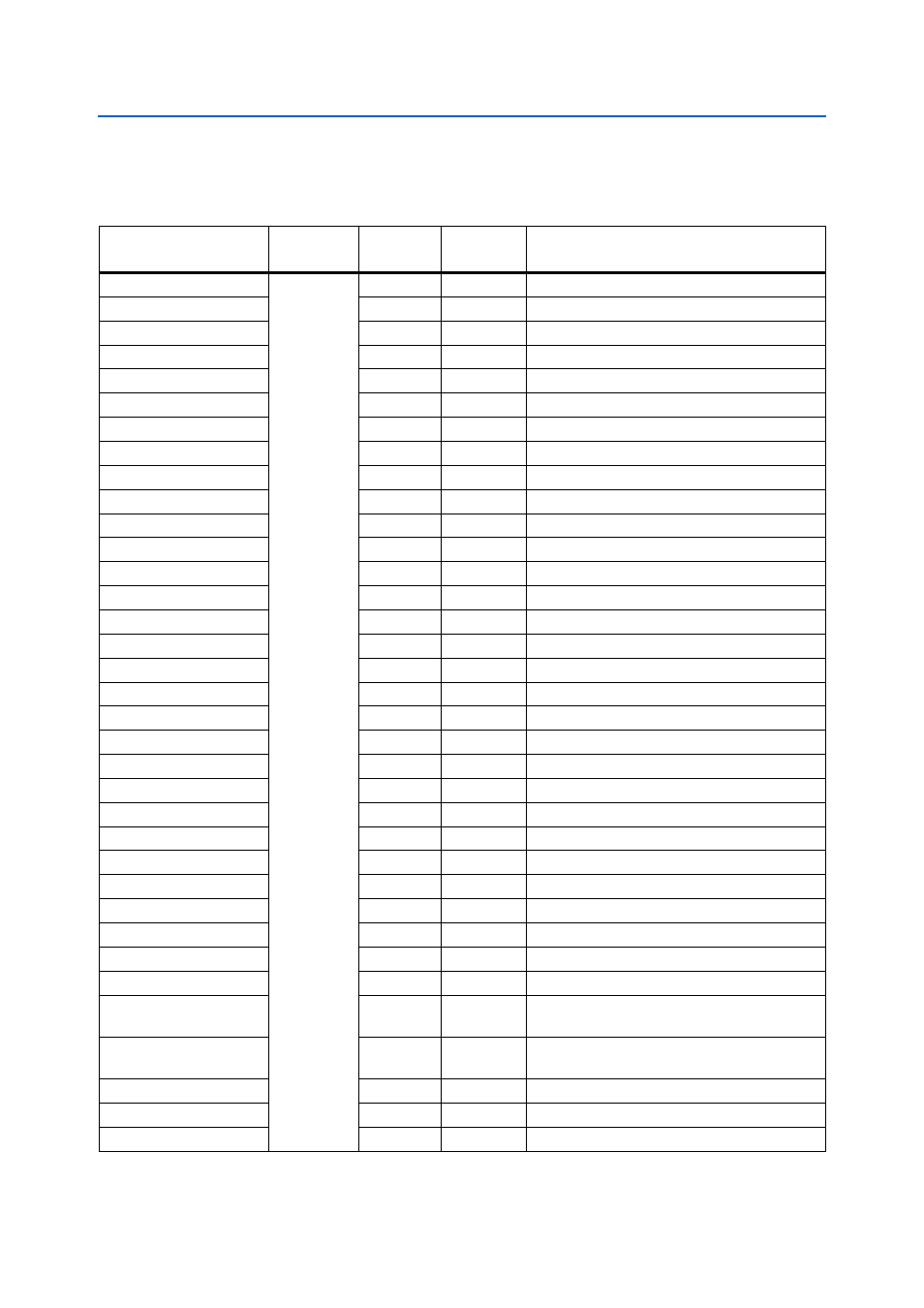
lists the I/O signals present on the MAX
II CPLD EPM2210 System
Controller. The signal names and functions are relative to the MAX
II device (U22).
Table 2–5. MAX II CPLD EPM2210 System Controller Device Pin-Out (Part 1 of 4)
Schematic Signal Name
I/O Standard
EPM2210
Pin Number
EP3CLS200
Pin Number
Description
CLK50_EN
2.5-V
H16
—
50 MHz oscillator enable
CLK66_EN
H13
—
66.6 MHz oscillator enable
CLK_CONFIG
J12
—
100 MHz configuration clock input
CLK_ENABLE
N7
—
DIP - clock oscillator enable
CLK_SEL
T5
—
DIP - clock select SMA or oscillator
CLKIN_50
J5
—
50 MHz clock input
CPU_RESETn
R8
W27
FPGA reset push-button switch
CRC_ERROR
K5
P26
FPGA CRC error
CRC_ERROR_MAX
K12
—
CRC error LED
CRC_ERROR_PB
R16
—
CRC error insert push-button switch
CRC_LATCH_SIG
K4
AF5
Anti-Tamper FPGA general I/O
FLASH_ADVn
B3
AF18
FSM bus flash memory address valid
FLASH_CEn
E6
AH22
FSM bus flash memory chip enable
FLASH_CLK
C6
AH6
FSM bus flash memory clock
FLASH_OEn
B4
AD7
FSM bus flash memory output enable
FLASH_RDYBSYn
D6
V4
FSM bus flash memory ready
FLASH_RESETn
C4
AH5
FSM bus flash memory reset
FLASH_WEn
A4
AH17
FSM bus flash memory write enable
FPGA_CONF_DONE
J1
P22
FPGA configuration done
FPGA_CONFIG_D0
D3
K1
FPGA configuration data
FPGA_DCLK
H4
L6
FPGA configuration clock
FPGA_EPM2210_TCK
C15
—
FPGA JTAG TCK
FPGA_EPM2210_TDI
E13
—
FPGA JTAG TDI
FPGA_EPM2210_TDO
E14
—
FPGA JTAG TDO
FPGA_EPM2210_TMS
C14
—
FPGA JTAG TMS
FPGA_INIT_DONE
N5
P27
FPGA INIT_DONE signal
FPGA_nCONFIG
T2
M3
FPGA configuration active
FPGA_nSTATUS
H3
M1
FPGA configuration ready
FPGA_TCK
P14
—
Anti-Tamper example design JTAG connector TCK
FPGA_TDI
P15
—
Anti-Tamper example design JTAG connector TDI
FPGA_TDO
M14
—
Anti-Tamper example design JTAG connector
TDO
FPGA_TMS
N13
—
Anti-Tamper example design JTAG connector
TMS
FSM_A0
C13
AG6
FSM bus address
FSM_A1
B16
AD14
FSM bus address
FSM_A2
C12
AA17
FSM bus address