Altera Cyclone III LS FPGA Development Board User Manual
Page 45
Chapter 2: Board Components
2–37
Memory
© October 2009 Altera Corporation
Cyclone III LS FPGA Development Board Reference Manual
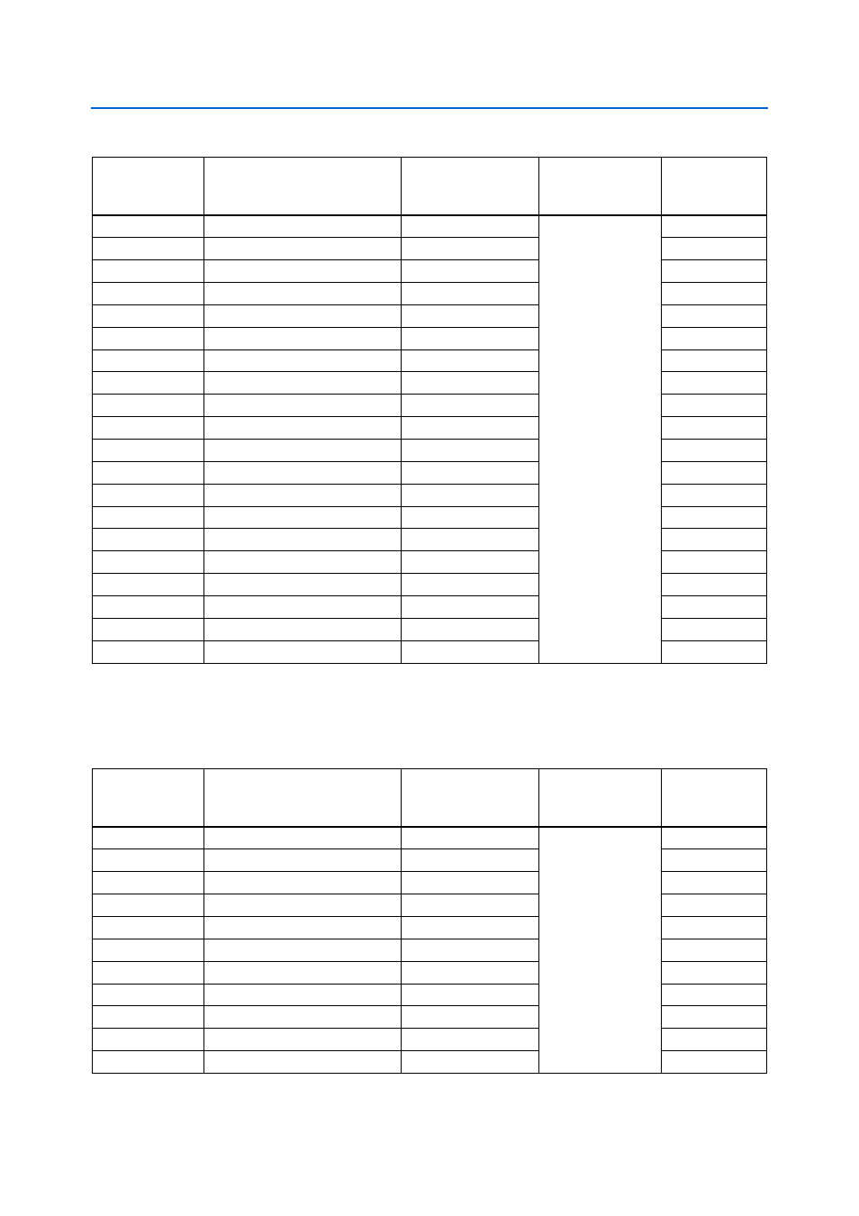
lists the DDR2 bank 8 pin assignments, signal names, and its functions. The
signal names and types are relative to the Cyclone III LS device in terms of I/O setting
and direction.
U6.F3
Write mask byte lane 0
DDR2_DM0
1.8-V SSTL Class I
C22
U6.B3
Write mask byte lane 1
DDR2_DM1
B25
U6.G8
Data bus byte lane 0
DDR2_DQ0
G20
U6.G2
Data bus byte lane 0
DDR2_DQ1
B19
U6.H7
Data bus byte lane 0
DDR2_DQ2
B21
U6.H3
Data bus byte lane 0
DDR2_DQ3
G19
U6.H1
Data bus byte lane 0
DDR2_DQ4
C19
U6.H9
Data bus byte lane 0
DDR2_DQ5
A21
U6.F1
Data bus byte lane 0
DDR2_DQ6
B18
U6.F9
Data bus byte lane 0
DDR2_DQ7
B22
U6.C8
Data bus byte lane 1
DDR2_DQ8
A26
U6.C2
Data bus byte lane 1
DDR2_DQ9
B27
U6.D7
Data bus byte lane 1
DDR2_DQ10
D23
U6.D3
Data bus byte lane 1
DDR2_DQ11
D22
U6.D1
Data bus byte lane 1
DDR2_DQ12
F21
U6.D9
Data bus byte lane 1
DDR2_DQ13
A25
U6.B1
Data bus byte lane 1
DDR2_DQ14
E21
U6.B9
Data bus byte lane 1
DDR2_DQ15
A27
U6.F7
Data strobe P byte lane 0
DDR2_DQS0
C18
U6.B7
Data strobe P byte lane 1
DDR2_DQS1
E22
Table 2–37. DDR2 Bank 7 Pin Assignments, Signal Names and Functions (Part 2 of 2)
Board Reference
Description
Schematic Signal
Name
I/O Standard
Cyclone III LS
Device
Pin Number
Table 2–38. DDR2 Bank 8 Pin Assignments, Signal Names and Functions (Part 1 of 2)
Board Reference
Description
Schematic Signal
Name
I/O Standard
Cyclone III LS
Device
Pin Number
U5.M8
Address bus
DDR2_B8_A0
1.8-V SSTL Class I
C5
U5.M3
Address bus
DDR2_B8_A1
F7
U5.M7
Address bus
DDR2_B8_A2
E5
U5.N2
Address bus
DDR2_B8_A3
G12
U5.N8
Address bus
DDR2_B8_A4
C4
U5.N3
Address bus
DDR2_B8_A5
D10
U5.N7
Address bus
DDR2_B8_A6
D5
U5.P2
Address bus
DDR2_B8_A7
B4
U5.P8
Address bus
DDR2_B8_A8
A5
U5.P3
Address bus
DDR2_B8_A9
C9
U5.M2
Address bus
DDR2_B8_A10
E10