Bidirectional configuration – Altera Double Data Rate I/O User Manual
Page 9
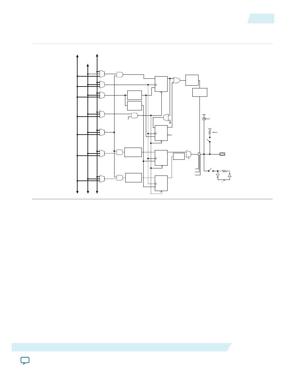
Figure 4: Stratix IOE in DDR Output I/O Configuration
This figure shows the IOE configuration for DDR outputs in Stratix series devices
CLRN/PRN
D
Q
ENA
Chip-Wide Reset
OE Register
CLRN/PRN
D
Q
ENA
OE Register
CLRN/PRN
D
Q
ENA
Output Register
VCCIO
VCCIO
Optional
PCI Clamp
Programmable
Pull-Up
Resistor
Column or Row
Interconnect
I/O Interconnect
[15..0]
IOE_CLK[7..0]
Bus-Hold
Circuit
Logic Array
to Output
Register Delay
Output
tZX Delay
OE Register
tCO Delay
CLRN/PRN
D
Q
ENA
Output Register
Logic Array
to Output
Register Delay
Drive Strength Control
Open-Drain Output
Slew Control
Used for
DDR SDRAM
clk
sclr
aclr/prn
clkout
Output
Pin Delay
Output
Enable Clock
Enable Delay
Output Clock
Enable Delay
Bidirectional Configuration
Input and output registers are independent of each other, enabling the bidirectional DDR I/O path to be
implemented entirely in the I/O element for Stratix, Stratix GX, and APEX II devices. The bidirectional
configuration includes an input path, an output path, and two output enable registers.
The bidirectional path consists of two data flow paths:
• Input path active
• Output path active
When the input path is active, the output enable disables the tri-state buffer, which prevents data from
being sent out on the output path. Disabling the tri-state buffer prevents contention at the I/O pin. The
input path behaves like the input configuration as shown in Figure 3–1 on page 3–1. When the output
path is active, the output enable register AOE controls the flow of data from the output registers. During
outgoing transactions, the bidirectional configuration behaves like the output configuration as shown in
Figure 3–3 on page 3–3. The second output enable register (B
OE
) is used for DDR SDRAM interfaces. This
negative-edge register extends the high-impedance state of the pin by a half clock cycle. This option is
useful to provide the write preamble for the DQS strobe in the DDR SDRAM interfaces. This feature is
enabled by using the Delay switch-on by a half clock cycle option in the ALTDDIO_BIDIR IP core in the
Quartus II software. You can bypass the input registers and latch to get a combinational output (
combout
)
from the pin going into the APEX II or Stratix series device. Furthermore, the input data ports
UG-DDRMGAFCTN
2015.01.23
Bidirectional Configuration
9
Double Data Rate I/O (ALTDDIO_IN, ALTDDIO_OUT, and ALTDDIO_BIDIR) IP Cores User Guide
Altera Corporation