Ddr i/o timing, The output of latch c, And the output of register a – Altera Double Data Rate I/O User Manual
Page 11: And b
•
For more information about the DDR registers in Cyclone devices
DDR I/O Timing
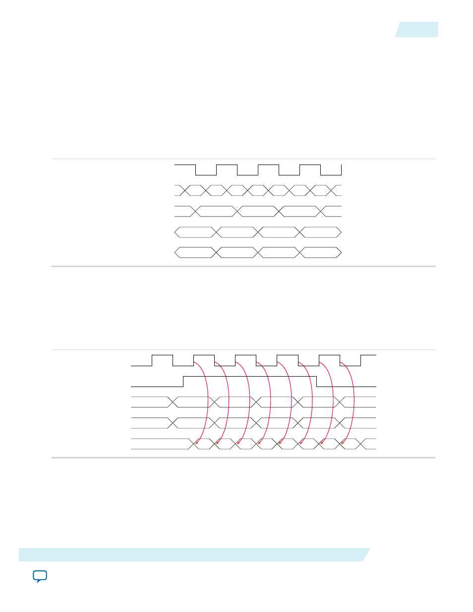
This figure shows the functional timing waveform for the input path. The signal names are the port names
used in the ALTDDIO_IN IP core. The
datain
signal is the input from the pin to the DDR circuitry. The
output of register B
I
is
neg_reg_out
. The output of latch C
I
is
dataout_1
, and the output of register A
I
is
dataout_h
.
dataout_h
and
dataout_l
feed the logic array and show the conversion of the data from a
DDR implementation to positive-edge triggered data.
Figure 6: DDR I/O Input Timing Waveform
inclock
datain
dataout_h
dataout_l
E0
E1
E2
D0
D1
D2
XX
XX
D0
D1
D2
E0
D0
E1
D1
E2
D2
D3
D3
XX
neg_reg_out
This figure shows a functional timing waveform example for the output path with the output enable
registered. In this example, the delay switch-on by a half clock cycle is not turned on, so the second
output enable register (B
OE
) is not used. The output enable signal OE is active high and can be driven
from a pin or internal logic. The data signals
datain_l
and
datain_h
are driven from the logic array to
output registers A
O
and B
O
. The
dataout
signal is the output from the DDR circuitry to the pin.
Figure 7: DDR I/O Output Timing Waveform
outclock
datain_l
dataout
datain_h
OE
D1
E1
D3
E3
D2
E2
D0
E0
ZZ
ZZ
D0
D1
D2
D3
XX
XX
E0
E1
E2
E3
XX
XX
The waveform in this figure reflects the software simulation results. The OE signal is active low in silicon;
however, the Quartus II software implements this as active high and automatically adds an inverter before
the D input of the OE register A
OE
. You can change the OE back to active low, if desired.
UG-DDRMGAFCTN
2015.01.23
DDR I/O Timing
11
Double Data Rate I/O (ALTDDIO_IN, ALTDDIO_OUT, and ALTDDIO_BIDIR) IP Cores User Guide
Altera Corporation