Verilog hdl prototype, Vhdl component declaration, Vhdl library-use declaration – Altera Double Data Rate I/O User Manual
Page 21: Document revision history
Name
Required
Description
oe_out
No
Output enable for the bidirectional
padio
port. Output
port [
WIDTH
–1..0] wide. This port is available for
Stratix III and Cyclone III devices only.
Table 10: ALTDDIO_BIDIR Bidirectional Port
Name
Required
Description
padio[]
Yes
Bidirectional DDR port that should directly feed a
bidirectional pin in the top-level design. The DDR data
is transmitted and received on this bidirectional port.
Bidirectional port
[(WIDTH) - (1)..0]
wide.
Verilog HDL Prototype
The Verilog HDL prototype is located in the
VHDL Component Declaration
You can locate VHDL component declaration in the VHDL Design File (.vhd)
altera_mf_components.vhd in the
directory.
VHDL LIBRARY-USE Declaration
The VHDL LIBRARY-USE declaration is not required if you use the VHDL Component Declaration.
LIBRARY altera_mf;
USE altera_mf.altera_mf_components.all;
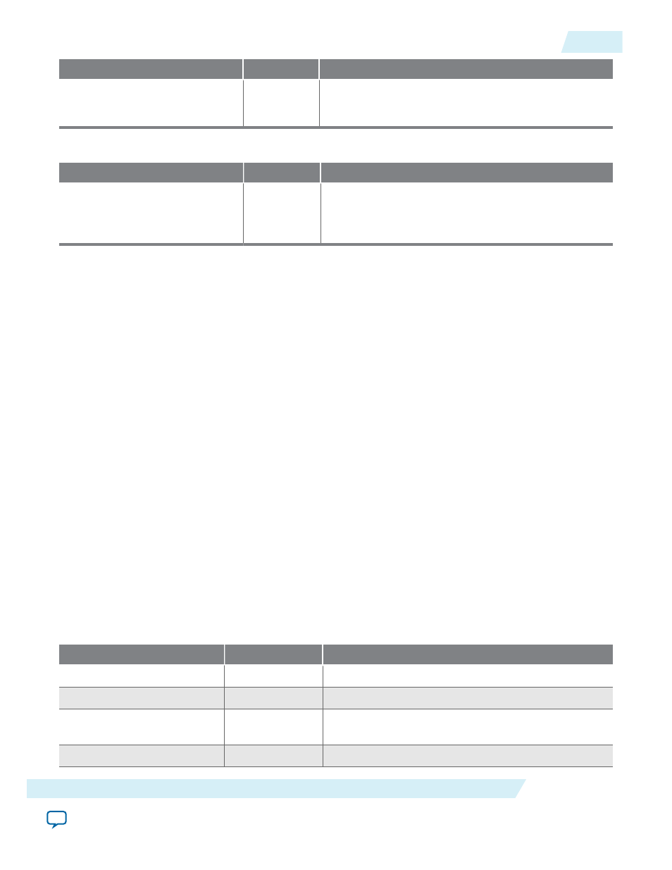
Document Revision History
The following table lists the revision history for this document.
Table 11: Document Revision History
Date
Version
Changes
January 2015
2015.01.23
Added link to design example file.
December 2014
2014.12.15
Template update.
January 2013
6.1
Updated to correct content error in “DDR I/O
Timing” on page 3–7.
February 2012
6.0
Updated to refelect new GUI changes.
UG-DDRMGAFCTN
2015.01.23
Verilog HDL Prototype
21
Double Data Rate I/O (ALTDDIO_IN, ALTDDIO_OUT, and ALTDDIO_BIDIR) IP Cores User Guide
Altera Corporation