Altddio_in ip core signals – Altera Double Data Rate I/O User Manual
Page 17
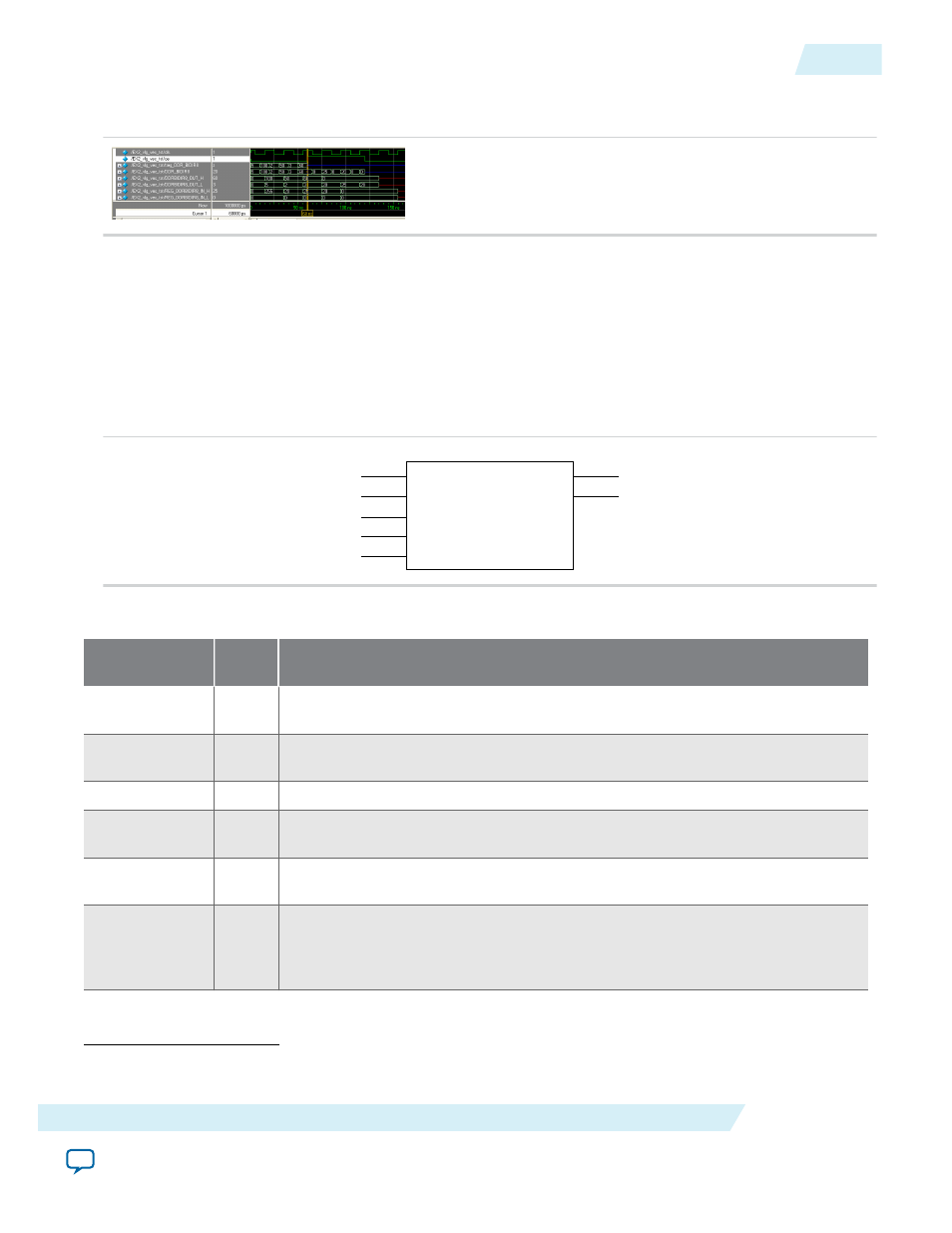
Figure 8: ModelSim Simulation Results
This figure shows the expected simulation results in ModelSim-Altera software.
Related Information
ALTDDIO_IN IP Core Signals
These tables list the input and output ports for the ALTDDIO_IN IP core.
Figure 9: ALTDDIO_IN Ports
datain[ ]
inclock
inclocken
aclr
aset
dataout_h[ ]
dataout_l[ ]
altddio_in
Table 4: ALTDDIO_IN Input Ports
Name
Require
d
Description
datain[]
Yes
DDR input data port. Input port
WIDTH
wide. The
datain
port should be directly
fed from an input pin in the top-level design.
inclock
Yes
Clock signal to sample the DDR input. The
datain
port is sampled on each clock
edge of the
inclock
signal.
inclocken
No
Clock enable for the data clock
aclr
No
Asynchronous clear input. The
aclr
and
aset
ports cannot be connected at the
same time.
aset
No
Asynchronous set input. The
aclr
and
aset
ports cannot be connected at the
same time.
sclr
No
Synchronous clear input. The
sclr
and
sset
ports cannot be connected at the
same time. The
sclr
port is available for Arria GX, Stratix III, Stratix II,
Stratix II GX, Stratix, Stratix GX, HardCopy II, and HardCopy Stratix devices
only.
(1)
(1)
When designing with Stratix III devices, when
sclr
is asserted, it synchronously presets both the input
path and resynchronization register.
UG-DDRMGAFCTN
2015.01.23
ALTDDIO_IN IP Core Signals
17
Double Data Rate I/O (ALTDDIO_IN, ALTDDIO_OUT, and ALTDDIO_BIDIR) IP Cores User Guide
Altera Corporation