Output configuration, And b – Altera Double Data Rate I/O User Manual
Page 7
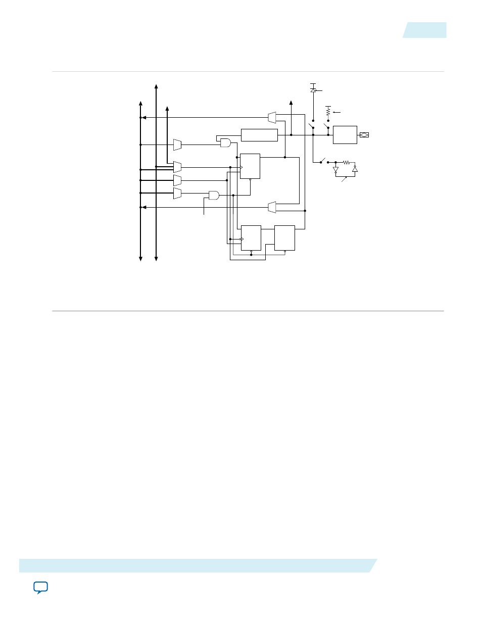
Figure 2: Stratix II IOE in DDR Input I/O Configuration
This figure shows an IOE configured for DDR inputs for a Stratix or Stratix II device.
CLRN/PRN
D
Q
ENA
Chip-Wide Reset
Input Register
CLRN/PRN
D
Q
ENA
Input Register
VCCIO
VCCIO
PCI Clamp
Programmable
Pull-Up
Resistor
Column, Row,
or Local
Interconnect
DQS Local
Bus
To DQS Logic
Block
ioe_clk[7..0]
Bus-Hold
Circuit
CLRN/PRN
D
Q
ENA
Latch
Input Pin to
Input RegisterDelay
sclr/spreset
clkin
aclr/apreset
On-Chip
Termination
ce_in
(2)
(3)
(4)
1) All input signals to the IOE can be inverted at the IOE.
2) This signal connection is only allowed on dedicated DQ function pins.
3) This signal is for dedicated DQS function pins only.
4) The optional PCI clamp is only available on column I/O pins.
Output Configuration
The dedicated output registers for Stratix series and APEX II devices are labeled A
O
and B
O
. These
positive-edge triggered registers and a multiplexer are used to implement the output path for DDR I/O.
UG-DDRMGAFCTN
2015.01.23
Output Configuration
7
Double Data Rate I/O (ALTDDIO_IN, ALTDDIO_OUT, and ALTDDIO_BIDIR) IP Cores User Guide
Altera Corporation