And b, This process doubles the data at the i/o pin – Altera Double Data Rate I/O User Manual
Page 8
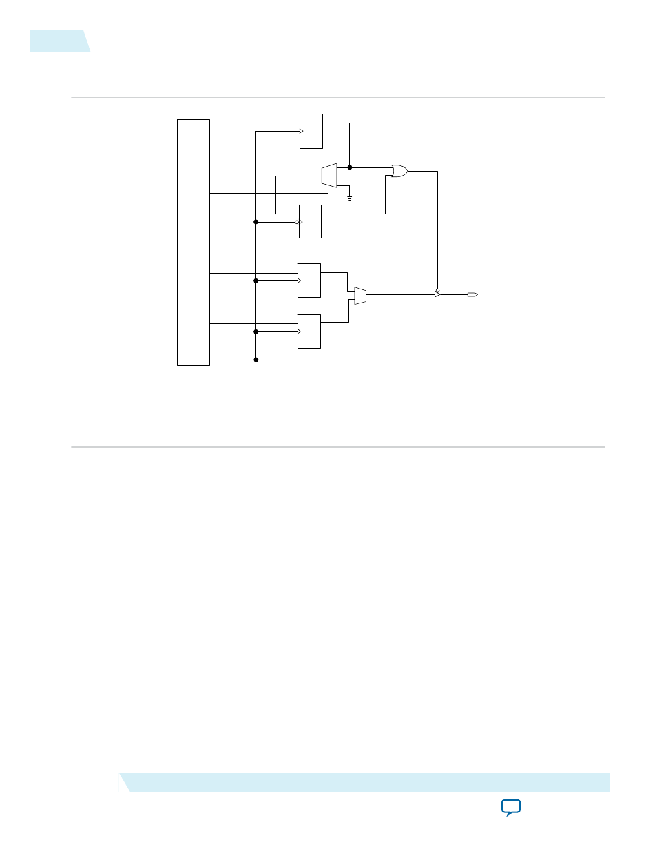
Figure 3: Output DDR I/O Path Configuration for Stratix Series and APEX II Devices
This figure shows the IOE configuration for DDR outputs in Stratix series and APEX II devices.
OUTPUT
Logic Array
outclock
datain_h
datain_l
D
Q
DFF
D
Q
DFF
0
1
Output Reg Ao
Output Reg Bo
D
Q
DFF
D
Q
DFF
OR2
TRI
dataout
OE Reg B
OE
OE Reg A
OE
0
1
(1)
OE
(2)
(4)
(3)
(5)
1) The OE is active low, but the Quartus II software implements this as active high and automatically adds an inverter before the input to the AOE
register during compilation. If desired, you can change the OE back to active low.
2) Register AOE generates the enable signal for general-purpose DDR I/O applications.
3) This select line corresponds to the delay switch-on by a half clock cycle option in the Parameter Editor.
4) Register BOE generates the delayed enable signal for DDR SDRAM applications.
5) The tri-state is active high by default. However, you can design it to be active low.
On the positive edge of the clock, a high data bit and a low data bit are captured in registers A
O
and B
O
.
The outputs of these two registers are fed to the input of a 2-to-1 multiplexer, which uses the output
register clock as its control signal. A high clock selects the data in register B
O
, and a low level of the clock
selects the data in register A
O
. This process doubles the data at the I/O pin.
8
Output Configuration
UG-DDRMGAFCTN
2015.01.23
Altera Corporation
Double Data Rate I/O (ALTDDIO_IN, ALTDDIO_OUT, and ALTDDIO_BIDIR) IP Cores User Guide