Boundary scan jtag, 1 pin descriptions, 2 jtag architecture – Cirrus Logic CS5376A User Manual
Page 75: Pin descriptions 21.2. jtag architecture, Figure 40. jtag block diagram, Cs5376a
CS5376A
DS612F4
75
21.BOUNDARY SCAN JTAG
The CS5376A includes an IEEE 1149.1 boundary scan JTAG port to test PCB interconnections. Refer to
the IEEE 1149.1 specification for more information about boundary scan testing.
21.1 Pin Descriptions
TRST - Pin 1
Reset input for the test access port (TAP) controller and all boundary scan cells, active low. Connect to
GND to disable the JTAG port.
TMS - Pin 2
Serial input to select the JTAG test mode.
TCK - Pin 3
Clock input to the TAP controller.
TDI - Pin 4
Serial input to the scan chain or TAP controller.
TDO - Pin 5
Serial output from the scan chain or TAP controller.
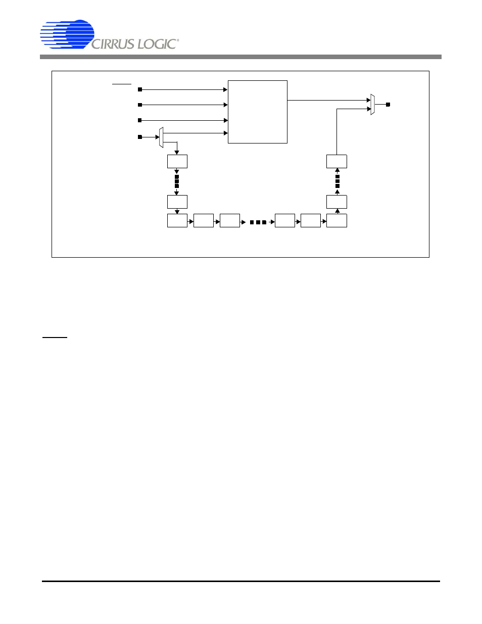
21.2 JTAG Architecture
The JTAG test circuitry consists of a test access port (TAP) controller and boundary scan cells connected
to each pin. The boundary scan cells are linked together to create a scan chain around the CS5376A.
Figure 40. JTAG Block Diagram
TDI
TDO
Controller
TAP
TRST
TMS
TCK
Boundary Scan Cells