Modulator interface, 1 pin descriptions, 2 modulator clock generation – Cirrus Logic CS5376A User Manual
Page 39: 3 modulator synchronization, Figure 20. modulator data interface, Cs5376a
CS5376A
DS612F4
39
10.MODULATOR INTERFACE
The CS5376A performs digital filtering for up to
four
∆Σ modulators. Signals from the modulators
are connected through the modulator data interface
(MDI).
10.1 Pin Descriptions
MCLK, MCLK/2 - Pins 13, 12
Modulator clock outputs. Nominally 2.048 MHz
and 1.024 MHz.
MSYNC - Pin 14
Modulator synchronization signal output. Generat-
ed from the SYNC input.
MDATA1 - MDATA4 - Pins 15, 17, 19, 21
Modulator data inputs, nominally 512 kbit/s.
MFLAG1 - MFLAG4 - Pins 16, 18, 20, 22
Modulator flag inputs. Driven high when modula-
tor is unstable due to an analog over-range signal.
10.2 Modulator Clock Generation
The MCLK and MCLK/2 outputs are low-jitter,
low-skew modulator clocks generated from the
32.768 MHz master clock.
MCLK typically operates at 2.048 MHz unless an-
alog low-power modes require a 1.024 MHz mod-
ulator clock. MCLK/2 always produces a clock at
half the selected MCLK rate.
The MCLK rate is selected and the MCLK and
MCLK/2 outputs are enabled by bits in the digital
filter CONFIG register (0x00). By default MCLK
and MCLK/2 are disabled and driven low.
10.3 Modulator Synchronization
The MSYNC output signal follows an input on the
SYNC pin. MSYNC phase aligns the modulator
sampling instant to guarantee synchronous analog
sampling across a measurement network.
MSYNC is enabled by a bit in the CONFIG register
(0x00). By default SYNC inputs do not cause an
MSYNC output.
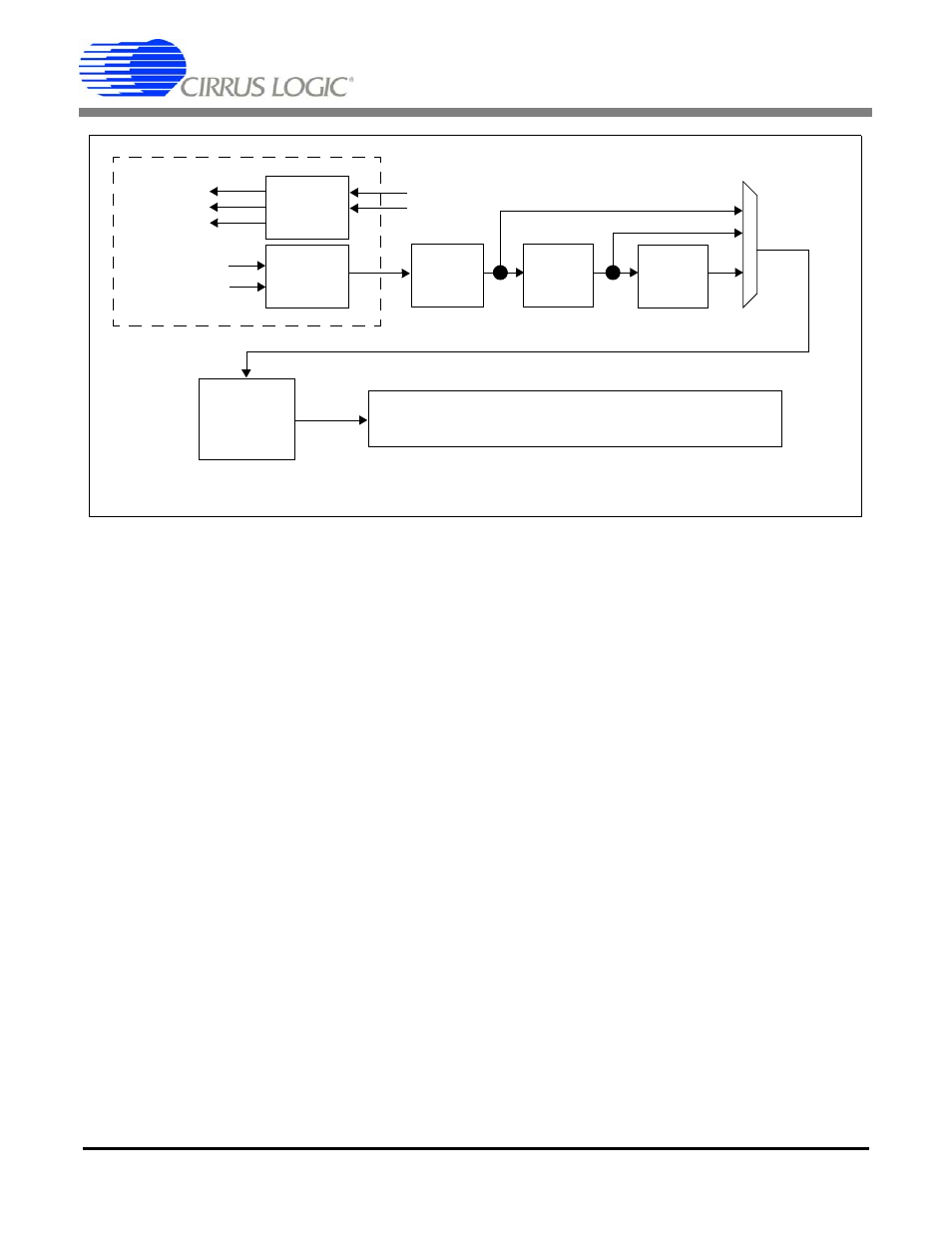
Figure 20. Modulator Data Interface
FIR
IIR
Filters
Filter
Output to High Speed Serial Data Port (SD Port)
DC Offset
Correction
Output Rate 4000 SPS ~ 1 SPS
& Gain
MDATA[4:1]
MFLAG[4:1]
MDI Input
512 kHz
MCLK /
Generate
MSYNC
CLK
SYNC
MSYNC
SINC
Filter
MCLK
MCLK/2