Clock generation, 1 pin description, 2 synchronous clocking – Cirrus Logic CS5376A User Manual
Page 24: 3 master clock jitter and skew, Figure 12. clock generation block diagram, Cs5376a
CS5376A
24
DS612F4
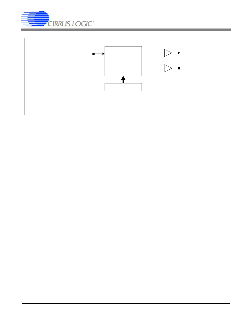
6. CLOCK GENERATION
The CS5376A requires a 32.768 MHz master clock
input, which is used to generate internal digital fil-
ter clocks and external modulator clocks.
6.1 Pin Description
CLK - Pin 58
Clock input, nominal frequency 32.768 MHz.
6.2 Synchronous Clocking
To guarantee synchronous measurements through-
out a sensor network, the CS5376A master clock
should be distributed to arrive at all nodes in phase.
The 32.768 MHz master clock can either be direct-
ly distributed through the system telemetry, or re-
constructed locally using a VCXO based PLL. To
ensure recovered clocks have identical phase, sys-
tem PLL designs should use a phase/frequency de-
tector architecture.
6.3 Master Clock Jitter and Skew
Care must be taken to minimize jitter and skew in
the received master clock as both parameters affect
measurement performance.
Jitter in the master clock causes jitter in the gener-
ated modulator clocks, resulting in sample timing
errors and increased noise.
Skew in the master clock from node to node creates
a sample timing offset, resulting in systematic mea-
surement errors in the reconstructed signal.
Clock Divider
CLK
DSPCFG Register
MCLK
Internal
Clocks
Figure 12. Clock Generation Block Diagram
and
Generator
MCLK
Output