Cirrus Logic CS5376A User Manual
Cs5376a low-power, multi-channel decimation filter, Features, Description
Copyright
© Cirrus Logic, Inc. 2008
(All Rights Reserved)
CS5376A
Low-power, Multi-channel Decimation Filter
Features
z
1- to 4-channel Digital Decimation Filter
Multiple On-chip FIR and IIR Coefficient Sets
Programmable Coefficients for Custom Filters
Synchronous Operation
z
Selectable Output Word Rate
4000, 2000, 1000, 500, 333, 250 SPS
200, 125, 100, 50, 40, 25, 20, 10, 5, 1 SPS
z
Digital Gain and Offset Corrections
z
Test DAC Bit-stream Generator
Digital Sine Wave Output
z
Time Break Controller, General Purpose I/O
z
Secondary SPI™ Port, Boundary Scan JTAG
z
Microcontroller or EEPROM Configuration
z
Small-footprint, 64-pin TQFP Package
z
Low Power Consumption
9 mW per Channel at 500 SPS
z
Flexible Power Supplies
I/O Interface: 3.3 V or 5.0 V
Digital Logic Core: 3.0 V, 3.3 V or 5.0 V
Description
The CS5376A is a multi-function digital filter utilizing a
low-power signal processing architecture to achieve ef-
ficient filtering for up to four
∆Σ modulators. By
combining the CS5376A with CS3301A/02A differential
amplifiers, CS5371A/72A
∆Σ modulators, and the
CS4373A
∆Σ test DAC a synchronous, high-resolution,
self-testing, multi-channel measurement system can be
designed quickly and easily.
Digital filter coefficients for the CS5376A FIR and IIR fil-
ters are included on-chip for a simple setup, or they can
be programmed for custom applications. Selectable dig-
ital filter decimation ratios produce output word rates
from 4000 SPS to 1 SPS, resulting in measurement
bandwidths ranging from 1600 Hz down to 400 mHz
when using the on-chip coefficient sets.
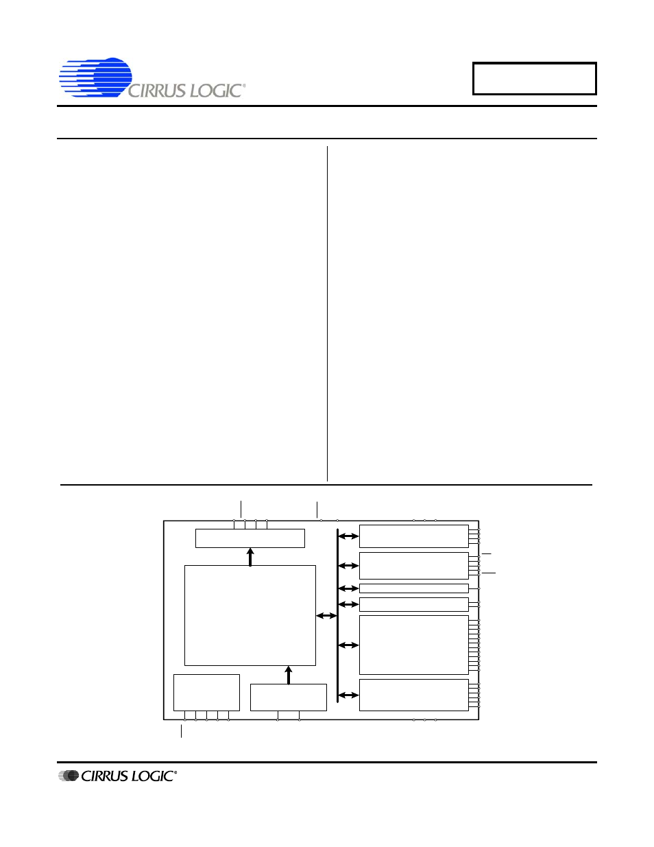
The CS5376A includes integrated peripherals to simplify
system design: offset and gain corrections, a test DAC
bit stream generator, a time-break controller, 12 gener-
al-purpose I/O pins, a secondary SPI port, and a
boundary scan JTAG port.
ORDERING INFORMATION
See
.
I
S C K 1
S e ria l D a ta O u tp u t P o rt
D e c im a tio n a n d
F ilte rin g E n g in e
M o d u la to r D a ta
In te rfa c e
T e s t B it S tre a m C o n tro lle r
C lo c k a n d
S yn c h ro n iz a tio n
T B S C L K
T B S D A T A
S P I 1
S e ria l P e rip h e ra l In te rfa c e 1
J T A G
In te rfa c e
T im e B re a k C o n tro lle r
S P I 2
S e ria l P e rip h e ra l In te rfa c e 2
G P IO
G e n e ra l P u rp o s e I/O
SDC
L
K
SDD
A
T
SDT
K
I
BO
O
T
VD (x
2)
VDD
1
VDD
2
(x
2)
S Y N C
C L K
M C L K
M S Y N C
T IM E B
M IS O
M O S I
S S I
S IN T
SDR
D
Y
S C K 2
S O
S I1
S I2
S I3
S I4
G P IO 1 1 :E E C S
G P IO 1 0
G P IO 9
G P IO 8
G P IO 7
G P IO 6
G P IO 5
G P IO 4 :C S 4
G P IO 3 :C S 3
G P IO 2 :C S 2
G P IO 1 :C S 1
G P IO 0 :C S 0
G
N
D (
x2)
G
N
D
2
(
x2)
GND1
M
D
ATA [
4
:1
]
MFLA
G [4
:1
]
TC
K
TM
S
TD
I
TDO
RESET
TRS
T
SEP ‘08
DS612F4
Document Outline
- Table of Contents
- List of Figures
- List of Tables
- 1. General Description
- 2. Characteristics and Specifications
- 3. System Design with CS5376A
- 4. Power Supplies
- 5. Reset Control
- 6. Clock Generation
- 7. Synchronization
- 8. Configuration By EEPROM
- 9. Configuration By Microcontroller
- 10. Modulator Interface
- 11. Digital Filter Initialization
- 12. SINC Filter
- 13. FIR Filter
- 14. IIR Filter
- 15. Gain and Offset Correction
- 16. Serial Data Port
- 17. Test Bit Stream Generator
- 18. Time Break Controller
- 19. General Purpose I/O
- 20. Serial Peripheral Interface 2
- 21. Boundary Scan JTAG
- 22. Device Revision History
- 23. Register Summary
- 24. Pin Descriptions
- 25. Package Dimensions
- 26. Ordering Information
- 27. Environmental, Manufacturing, & Handling Information
- 28. Revision History