Power supplies, 1 pin descriptions, Pin descriptions – Cirrus Logic CS5376A User Manual
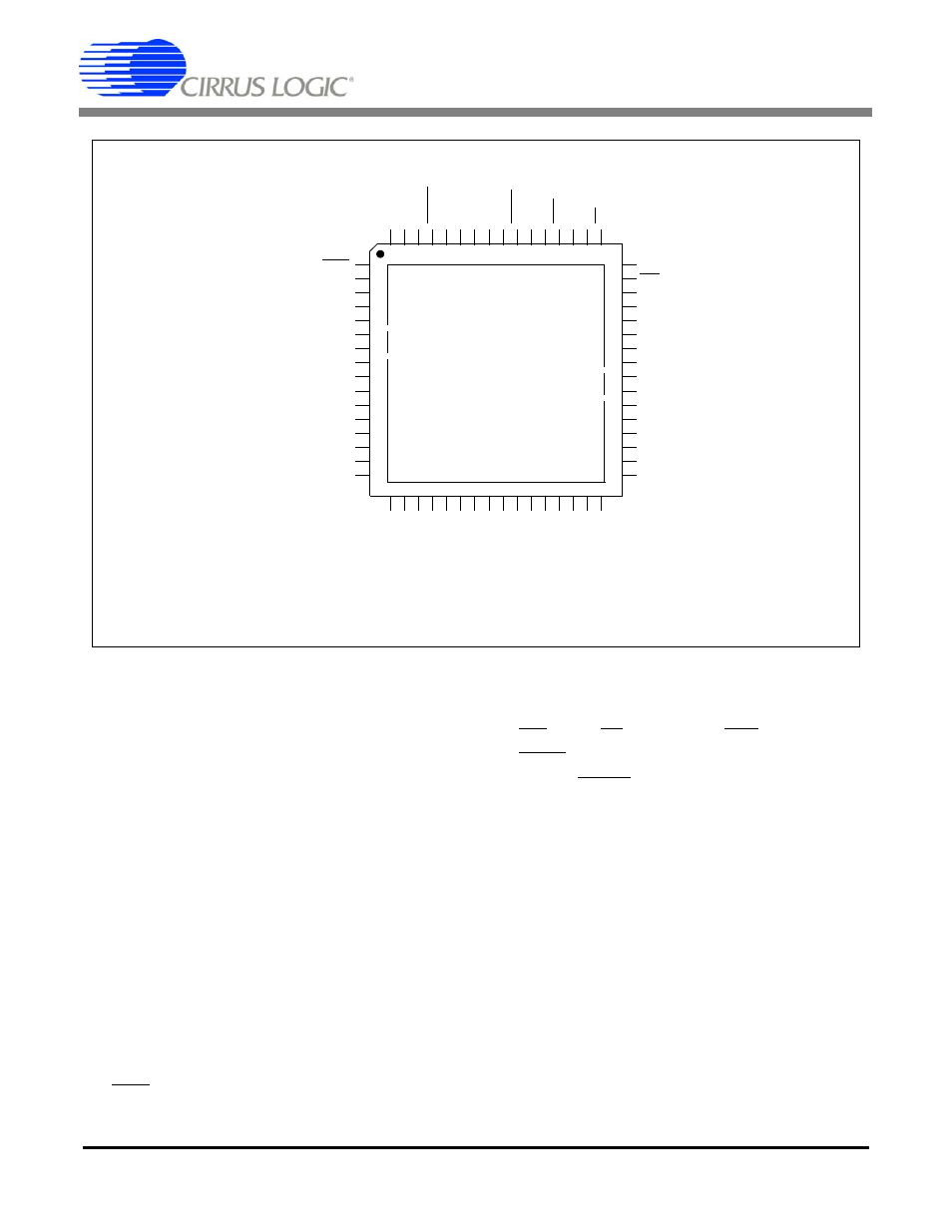
Page 21: Figure 10. power supply block diagram, Cs5376a
CS5376A
DS612F4
21
4. POWER SUPPLIES
The CS5376A has three sets of power supply in-
puts. Two sets supply power to the I/O pins of the
device (VDD1, VDD2), and the third supplies
power to the logic core (VD). The I/O pin power
supplies determine the maximum input and output
voltages when interfacing to peripherals, and the
logic core power supply largely determines the
power consumption of the CS5376A.
4.1 Pin Descriptions
VDD1, GND1 - Pins 54,53
Sets the interface voltage to a microcontroller and
system telemetry. Can be driven with voltages from
3.3 V to 5 V.
VDD1 powers pins 1-5 and 41-64:
TRST, TMS, TCK, TDI, TDO
GPIO6 - GPIO11:EECS
SSO, SCK1, SSI, MISO, MOSI, SINT,
RESET, BOOT, TIMEB, CLK, SYNC
SDDAT, SDRDY, SDCLK, SDTKO, SDTKI
VDD2, GND2 - Pins 11, 25, 24, 38
Sets the interface voltage to the modulators, test
DAC, and serial peripherals. Can be driven with
voltages from 3.3 V to 5 V.
VDD2 powers pins 8-37:
TBSCLK, TBSDATA
MCLK/2, MCLK, MSYNC
MDATA1 - MDATA4
MFLAG1 - MFLAG4
SI1 - SI4, SO, SCK2
GPIO0:CS0 - GPIO5
TRST
TMS
TCK
TDI
TDO
GND
VD
TBSCLK
TBSDATA
DNC
VDD2
MCLK/2
MCLK
MSYNC
MDATA4
MFLAG4
1
2
3
4
5
6
7
8
9
10
11
12
13
14
15
16
48
47
46
45
44
43
42
41
40
39
38
37
36
35
34
33
17 18 19 20 21 22 23 24 25 26 27 28 29 30 31 32
64 63 62 61 60 59 58 57 56 55 54 53 52 51 50 49
MDA
T
A3
MFLAG3
MDA
T
A2
MFLAG2
MDA
T
A1
MFLAG1
GND
GND2
VDD2
SI
4
SI
3
SI
2
SI
1
SO
SC
K2
G
P
IO0:
C
S
0
SDTKI
SDTKO
SDCLK
SDRDY
SDDA
T
SYNC
CLK
TIM
E
B
BOOT
RESET
VDD1
GND1
SINT
MO
SI
MIS
O
SSI
CS5376A
VDD1 Pad Ring
VDD2 Pad Ring
VD
Pad Ring
SCK1
SSO
GPIO11:EECS
GPIO10
GPIO9
GPIO8
GPIO7
GPIO6
VD
GND
GND2
GPIO5
GPIO4:CS4
GPIO3:CS3
GPIO2:CS2
GPIO1:CS1
VD
Pad Ring
Figure 10. Power Supply Block Diagram