Characteristics and specifications, Ac & dc parametric specifications, Recommended operating conditions – Cirrus Logic CS4955 User Manual
Page 6: Thermal characteristics, Dc characteristics
CS4954 CS4955
6
DS278F6
1. CHARACTERISTICS AND SPECIFICATIONS
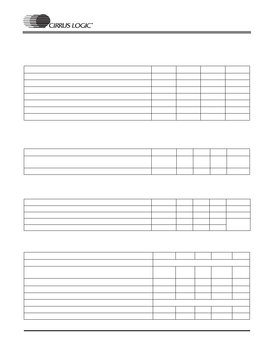
ABSOLUTE MAXIMUM RATINGS
AC & DC PARAMETRIC SPECIFICATIONS
(AGND,DGND = 0 V, all voltages with respect to 0 V)
WARNING: Operating beyond these limits can result in permanent damage to the device. Normal operation is not
guaranteed at these extremes.
RECOMMENDED Operating Conditions
(AGND,DGND = 0 V, all voltages with respect to 0 V.)
Note:
Operation outside the ranges is not recommended.
THERMAL CHARACTERISTICS
Note:
Four-layer PCB recommended for operation in environments where TA > 70° C.
DC CHARACTERISTICS
(T
A
= 25° C; VAA, VDD = 5 V; GNDA, GNDD = 0 V.)
Parameter
Symbol
Min
Max
Units
Power Supply
VAA/VDD
-0.3
6.0
V
Input Current Per Pin (Except Supply Pins)
-10
10
mA
Output Current Per Pin (Except Supply Pins)
-50
+50
mA
Analog Input Voltage
-0.3
VAA + 0.3
V
Digital Input Voltage
-0.3
VDD + 0.3
V
Ambient Temperature Power Applied
-55
+ 125
°C
Storage Temperature
-65
+ 150
°C
Parameter
Symbol
Min
Typ
Max
Units
Power Supplies: Digital Analog
VAA/VDD
3.15
4.75
3.3
5.0
3.45
5.25
V
Operating Ambient Temperature
TA
-40
+25
+85
°C
Parameters
Symbol
Min
Typ
Max
Units
Allowable Junction Temperature
-
-
150
°C
Junction to Ambient Thermal Impedance
-
-
-
(Four-layer PCB) TQFP
θ
JA-TM
-
45
-
°C/W
(Two-layer PCB) TQFP
θ
JA-TS
-
65
-
Parameter
Symbol
Min
Typ Max Units
Digital Inputs
High level Input Voltage
V [7:0], PDAT [7:0], Hsync/Vsync/CLKIN
VIH
2.2
-
VDD+0.3
V
High Level Input Voltage I²C
VIH
0.7 VDD
-
-
V
Low level Input Voltage All Inputs
-
-0.3
-
0.8
V
Input Leakage Current
-
-10
-
+10
μA
Digital Outputs
High Level Output Voltage lo = -4 mA
VOH
2.4
-
VDD
V
Low level Output Voltage lo = 4 mA
VOL
-
-
0.4
V