7 dac useage rules, Programming, 1 host control interface – Cirrus Logic CS4955 User Manual
Page 34: 1 i·c® interface, Host control interface, 1 i²c® interface
CS4954 CS4955
34
DS278F6
current flow from the output. To completely dis-
able or for low power device operation, the blue
DAC can be totally shut down via the B_PD con-
trol register bit in Control Register 4 (0×04). In this
mode turn-on using the control register will not be
instantaneous.
7.4.7 DAC Useage Rules
If some of the 6 DACs are not used, it is strongly
recommended to power them down (see
CONTROL_4 register) in order to reduce the pow-
er dissipation.
Depending on the external resistor connected to the
ISET pin the output drive of the DACs can be
changed. An external resistor of 4 k
Ω must be con-
nected to the ISET pin for normal operation.
There are two outpout impedance modes that the
DACs can be operated in. The first mode is the high
impedance mode (LOW_IMP bit set to 0). In this
mode, the DAC output drives a double terminated
300
Ω
load and will output a video signal which
conforms to the proper analog video specifications.
External buffers will be needed if the DAC output
load differs from a double terminated 300
Ω
load.
The second mode is the low impedence mode
(LOW_IMP but set to 1). In this mode, the DAC
output drives a double terminated 75
Ω
load
and
will output a video signal which conforms to the
proper analog video specifications. No external
buffers are necessary. The ouputs can directly drive
a television input.
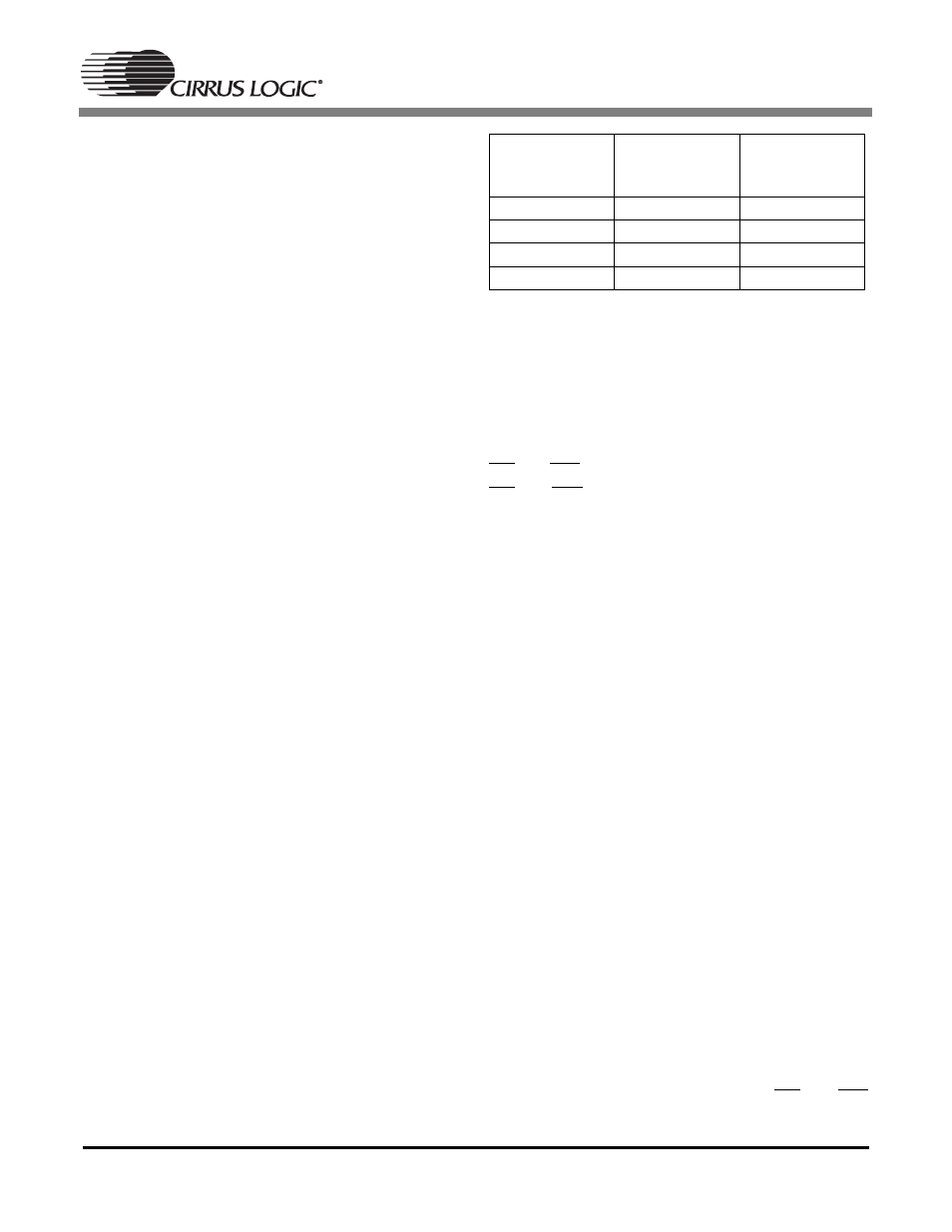
Note that for power dissipation purposes it is not
always possible to have all the 6 DACs active at the
same time. Table
shows the maximum number of
active DACs allowed depending on the power sup-
ply and low/high impedance modes. If less than 6
DACs are allowed to be active, the other DACs
must be powered down (see CONTROL_4 regis-
ter).
8.
PROGRAMMING
8.1
Host Control Interface
The CS4954/5 host control interface can be config-
ured for I²C or 8-bit parallel operation. The
CS4954/5 will default to I²C operation when the
RD and WR pins are both tied low at power up. The
RD and WR pins are active for 8-bit parallel oper-
ation only.
8.1.1 I²C
®
Interface
The CS4954/5 provides an I²C interface for access-
ing the internal control and status registers. Exter-
nal pins are a bidirectional data pin (SDA) and a
serial input clock (SCL). The protocol follows the
I²C specifications. A complete data transfer is
shown in Figure
. Note that this I²C interface
will work in Slave Mode only - it is not a bus mas-
ter.
SDA and SCL are connected via an external pull-
up resistor to a positive supply voltage. When the
bus is free, both lines are high. The output stages of
devices connected to the bus must have an open-
drain or open-collector in order to perform the
wired-AND function. Data on the I²C bus can be
transferred at a rate of up to 400 Kbits/sec in fast
mode. The number of interfaces to the bus is solely
dependent on the limiting bus capacitance of 400
pF. When 8-bit parallel interface operation is being
used, SDA and SCL can be tied directly to ground.
The I²C bus address for the CS4954/5 is program-
mable via the I2C_ADR Register (0×0F). When
I²C interface operation is being used, RD and WR
Nominal Power
supply
Low/High
Impedance
mode
maximum # of
active DACs
3.3V
Low Impedance
3
3.3V
High Impedance
6
5.0V
Low Impedance
3
5.0V
High Impedance
6
Table 8. Maximum DAC Numbers