Sync register 1, I·c address register, Subcarrier amplitude register – Cirrus Logic CS4955 User Manual
Page 44: Subcarrier synthesis register
CS4954 CS4955
44
DS278F6
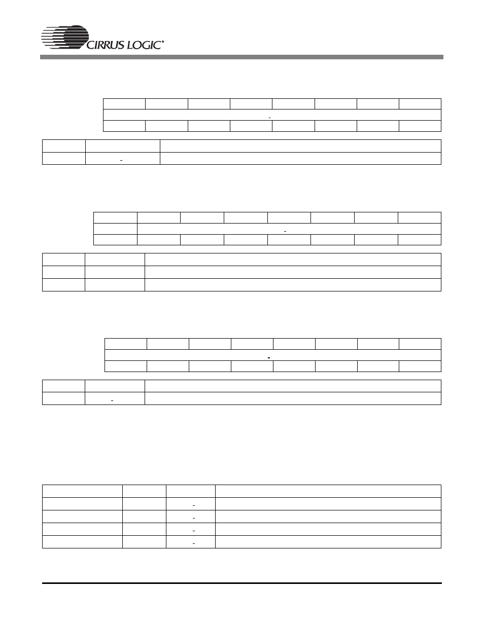
Sync Register 1
Address
0
×
0E
Sync_1
Read/Write
Default Value = F4h
I²C Address Register
Address
0
×
0F
I²C_ADR
Read/Write
Default Value = 00h
Subcarrier Amplitude Register
Address
0
×
10
SC_AMP
Read/Write
Default Value = 1Ch
Subcarrier Synthesis Register
Address
0
×
11
SC_SYNTH0
Read/Write
Default Value = 3Eh
0
×
12
SC_SYNTH1
F8h
0
×
13
SC_SYNTH2
E0h
0
×
14
SC_SYNTH3
43h
Bit Number
7
6
5
4
3
2
1
0
Bit Name
PROG HS[7:0]
Default
1
1
1
1
0
1
0
0
Bit
Mnemonic
Function
7:0
PROG HS[7:0]
programmable hsync pixels lsb
Bit Number
7
6
5
4
3
2
1
0
Bit Name
RESERVED
I²C ADR
Default
0
0
0
0
0
0
0
0
Bit
Mnemonic
Function
7
-
reserved
6:0
I²C
I²C device address (programmable)
Bit Number
7
6
5
4
3
2
1
0
Bit Name
BU AMP
Default
0
0
0
1
1
1
0
0
Bit
Mnemonic
Function
7:0
BU AMP
Color burst amplitude
Register
Bits
Mnemonic
Function
SC_SYNTH0
7:0
CC 0
Subcarrier synthesis bits 7:0
SC_SYNTH1
7:0
CC 1
Subcarrier synthesis bits 15:8
SC_SYNTH2
7:0
CC 2
Subcarrier synthesis bits 23:16
SC_SYNTH3
7:0
CC 3
Subcarrier synthesis bits 31:24