Cirrus Logic CS4955 User Manual
Features, Description, Programmable hsync and vsync timing

1
Copyright
© Cirrus Logic, Inc. 2006
(All Rights Reserved)
www.cirrus.com
CS4954
CS4955
NTSC/PAL Digital Video Encoder
Features
z
Six DACs providing simultaneous
composite,S-video, and RGB or Component
YUV outputs
z
Programmable DAC output currents for low
impedance (37.5
Ω) and high impedance
(150
Ω) loads
z
Multi-standard support for NTSC-M, NTSC-
JAPAN, PAL (B, D, G, H, I, M, N,
Combination N)
z
ITU R.BT656 input mode supporting
EAV/SAV codes and CCIR601 Master/Slave
input modes
z
Programmable HSYNC and VSYNC timing
z
Multistandard Teletext (Europe, NABTS,
WST) support
z
VBI encoding support
z
Wide-Screen Signaling (WSS) support, EIA-J
CPX1204
z
NTSC closed caption encoder with interrupt
z
CS4955 supports Macrovision copy
protection Version 7
z
Host interface configurable
for parallel or I²C
®
compatible
operation
z
On-chip voltage reference
generator
z
+3.3 V or +5 V operation,
CMOS, low-power modes,
three-state DACs
Description
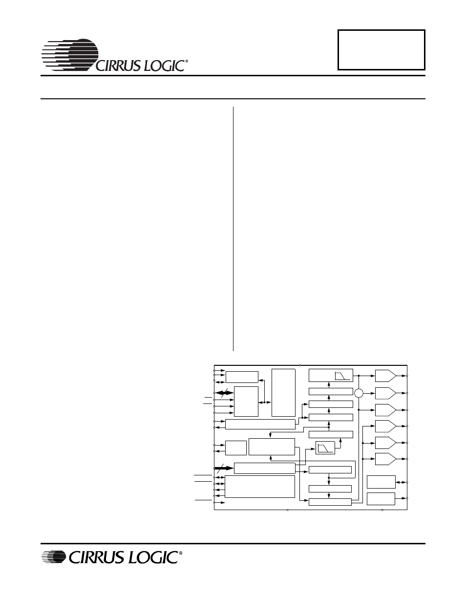
The CS4954/5 provides full conversion from digital video
formats YCbCr or YUV to NTSC and PAL Composite,
Y/C (S-video) and RGB, or YUV analog video. Input for-
mats can be 27 MHz 8-bit YUV, 8-bit YCbCr, or ITU
R.BT656 with support for EAV/SAV codes. Video output
can be formatted to be compatible with NTSC-M, NTSC-
J, PAL-B,D,G,H,I,M,N, and Combination N systems.
Closed Caption is supported in NTSC. Teletext is sup-
ported for NTSC and PAL.
Six 10-bit DACs provide two channels for an S-Video
output port, one or two composite video outputs, and
three RGB or YUV outputs. Two-times oversampling re-
duces the output filter requirements and guarantees no
DAC-related modulation components within the speci-
fied bandwidth of any of the supported video standards.
Parallel or high-speed I²C compatible control interfaces are
provided for flexibility in system design. The parallel interface
doubles as a general purpose I/O port when the CS4954/5 is
in I²C mode to help conserve valuable board area.
The CS4954 and CS4955 are available in a 48-pin TQFP
and operate in -40 to +85°C ambient temperature. The
CDB4954/55 Customer Demonstration board is also
available. Please refer to
.
SEPTEMBER '06
DS278F6
CLK
ISET
DGND
SCL
SDA
PDAT[7:0]
RD
WR
PADR
XTAL_OUT
VD[7:0]
HSYNC
VSYNC
FIELD
INT
RESET
I²C Interface
Host
Parallel
Interface
Color Sub-carrier Synthesizer
8
Video Formatter
Control
Registers
Chroma Modulate
Chroma Amplifier
Output
Interpolate
LPF
Burst Insert
Chroma Interpolate
LPF
Luma Interpolate
Luma Amplifier
Sync Insert
U,V
Y
Video Timing
Generator
TEST
Current
Reference
Voltage
Reference
VREF
R
DAC
Y
DAC
CVBS
DAC
C
10-Bit
DAC
Σ
VAA
XTAL_IN
Teletext
Encoder
TTXRQ
TTXDAT
YCbCr to RBG
B
DAC
G
DAC
10-Bit
10-Bit
10-Bit
10-Bit
10-Bit
RGB
RGB
Y
Y
8
Color Space
Converter
Document Outline
- 1. Characteristics and Specifications
- 2. Additional CS4954/5 Features
- 3. CS4954 Introduction
- 4. Functional Description
- 4.1 Video Timing Generator
- 4.2 Video Input Formatter
- 4.3 Color Subcarrier Synthesizer
- 4.4 Chroma Path
- 4.5 Luma Path
- 4.6 RGB Path and Component YUV Path
- 4.7 Digital to Analog Converters
- 4.8 Voltage Reference
- 4.9 Current Reference
- 4.10 Host Interface
- 4.11 Closed Caption Services
- 4.12 Teletext Services
- 4.13 Wide-Screen Signaling Support and CGMS
- 4.14 VBI Encoding
- 4.15 Control Registers
- 4.16 Testability
- 5. Operational Description
- 5.1 Reset Hierarchy
- 5.2 Video Timing
- 5.3 ITU-R.BT656
- 5.4 Digital Video Input Modes
- 5.5 Multi-standard Output Format Modes
- 5.6 Subcarrier Generation
- 5.7 Subcarrier Compensation
- 5.8 Closed Caption Insertion
- 5.9 Programmable H-sync and V-sync
- 5.10 Wide Screen Signaling (WSS) and CGMS
- 5.11 Teletext Support
- 5.12 Color Bar Generator
- 5.13 VBI encoding
- 5.14 Super White/Super Black support
- 5.15 Interrupts
- 5.16 General Purpose I/O Port
- 6. Filter Responses
- 7. Analog
- 8. Programming
- 8.1 Host Control Interface
- 8.2 Register Description
- 8.2.1 Control Registers
- Control Register 0
- Control Register 1
- Control Register 2
- Control Register 3
- Control Register 4
- Control Register 5
- Control Register 6
- Background Color Register
- GPIO Control Register
- GPIO Data Register
- Sync Register 0
- Sync Register 1
- I·C Address Register
- Subcarrier Amplitude Register
- Subcarrier Synthesis Register
- Hue LSB Adjust Register
- Hue MSB Adjust Register
- SCH Sync Phase Adjust
- Closed Caption Enable Register
- Closed Caption Data Register
- Wide Screen Signaling Register 0
- Wide Screen Signalling Register 1
- Wide Screen Signalling Register 2
- Filter Register 0
- Filter Register 1
- Filter Register 2
- Filter Register 3
- Filter Register 4
- Filter Register 5
- Filter Register 6
- Teletext Register 0
- teletext Register 1
- Teletext Register 2
- teletext Register 3
- Teletext Register 4
- teletext Register 5
- Teletext Register 6
- teletext Register 7
- teletext Register 8
- Interrupt Register 0
- Interrupt Register 1
- Status Register 0
- Status Register 1
- 9. Board Design And Layout Considerations
- 10. Pin Description
- 11. Package Drawing
- 12. Revision History
