2 8-bit parallel interface – Cirrus Logic CS4955 User Manual
Page 35
CS4954 CS4955
DS278F6
35
must be tied to ground. PDAT [7:0] are available to
be used for GPIO operation in I²C host interface
mode. For 3.3 V operation it is necessary to have
the appropriate level shifting for I²C signals.
8.1.2 8-bit Parallel Interface
The CS4954/5 is equipped with a full 8-bit parallel
microprocessor write and read control port. Along
with the PDAT [7:0] pins, the control port interface
is comprised of host read (RD) and host write (WR)
active low strobes and host address enable
(ADDR), which, when low, enables unique address
register accesses. The control port is used to access
internal registers which configure the CS4954/5 for
various modes of operation. The internal registers
are uniquely addressed via an address register. The
address register is accessed during a host write cy-
cle when the WR and ADDR pins set low. Host
write cycles with ADDR set high will write 8-bit
data to the PDAT [7:0] pins into the register cur-
rently selected by the address register. Likewise
read cycles occuring with RD set low and ADDR
set high will return the register contents selected by
the address register. Reference the detailed electri-
cal timing parameter section of this data sheet for
exact host parallel interface timing characteristics
and specifications.
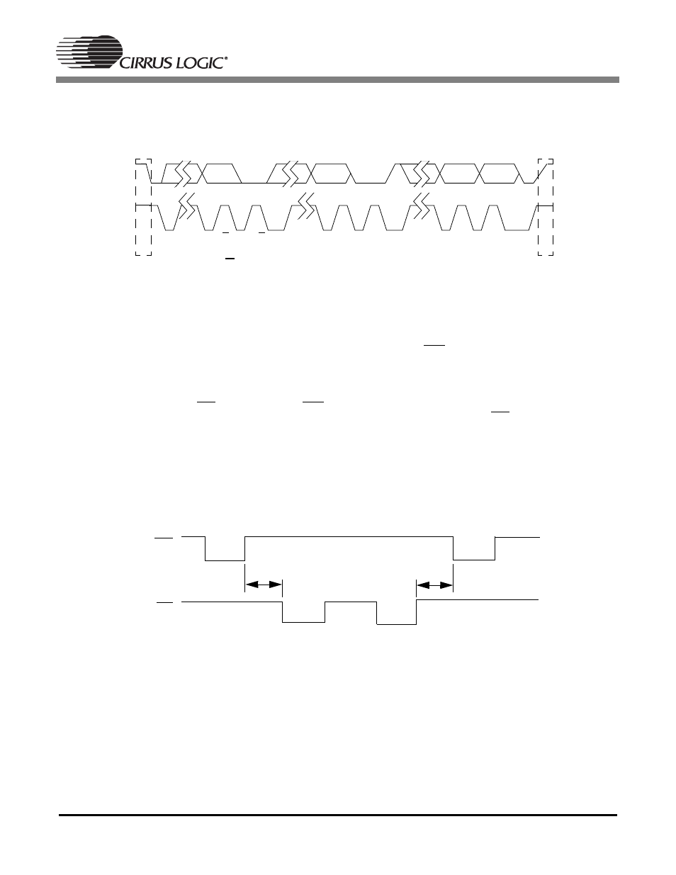
SDA
SCL
A
P
Start
Address
1-7
R/W
8
9
ACK
1-7
Data
8
9
1-7
8
9
ACK
Data ACK
Stop
Note: I²C transfers data always with MSB first, LSB last
Figure 26. I²C Protocol
T
rec
T
rec
WR
RD
Figure 27. 8-bit Parallel Host Port Timing: Read-Write/Write-Read Cycle