Background color register, Gpio control register, Gpio data register – Cirrus Logic CS4955 User Manual
Page 43: Sync register 0
CS4954 CS4955
DS278F6
43
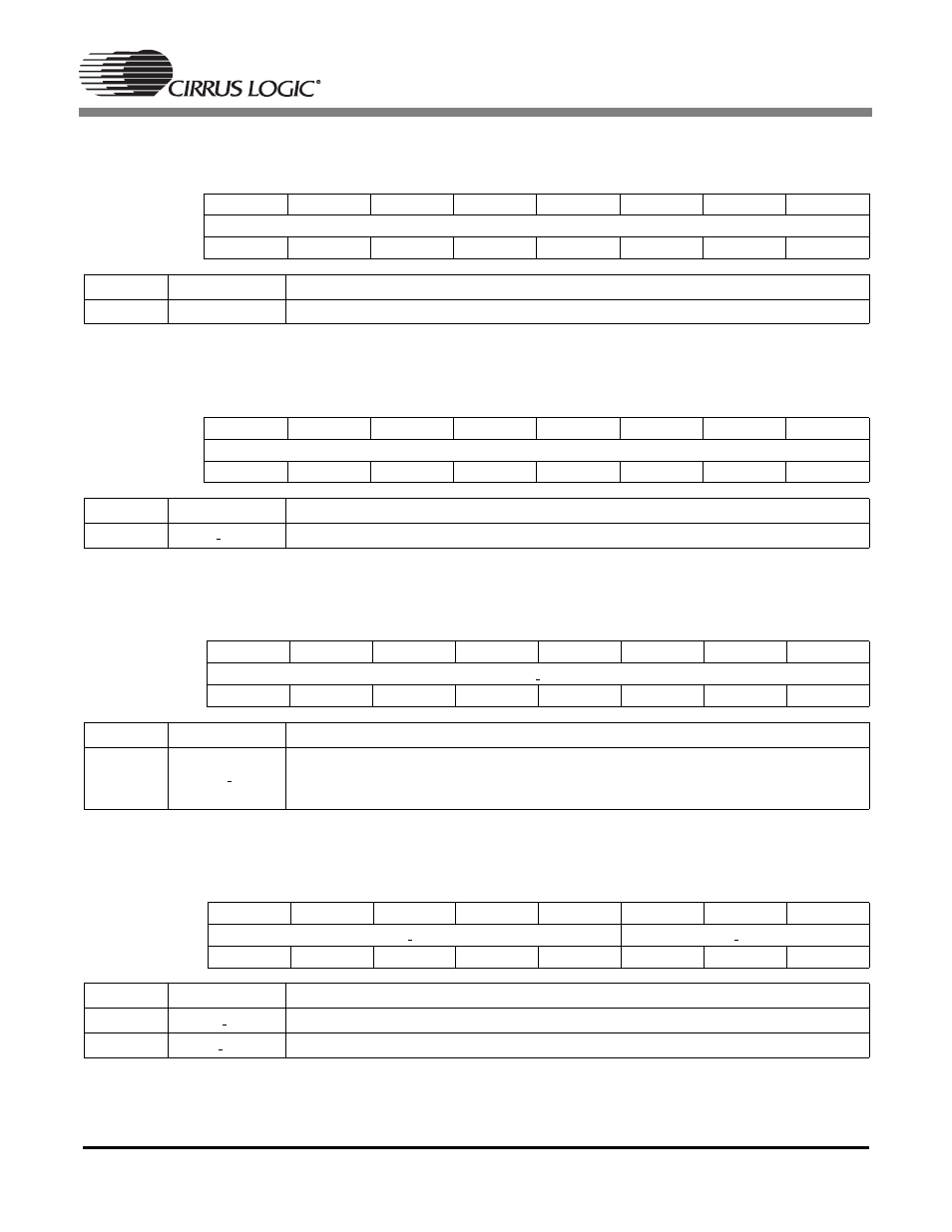
Background Color Register
Address
0
×
08
BKG_COLOR Read/Write
Default Value = 03h
GPIO Control Register
Address
0
×
09
GPIO__REG
Read/Write
Default Value = 00h
GPIO Data Register
Address
0
×
0A
GPIO_REG
Read/Write
Default Value = 00h
Sync Register 0
Address
0
×
0D
Sync_0
Read/Write
Default Value = 90h
Bit Number
7
6
5
4
3
2
1
0
Bit Name
BG
Default
0
0
0
0
0
0
1
1
Bit
Mnemonic
Function
7:0
BG
Background color (7:5 = R, 4:2 = G, 1:0 = B) (default is 0000 0011 - blue)
Bit Number
7
6
5
4
3
2
1
0
Bit Name
GPR_CNTRL
Default
0
0
0
0
0
0
0
0
Bit
Mnemonic
Function
7:0
GPR CNTRL
Input(0)/output(1) control of GPIO registers (bit 0: PDAT(0), bit 7: PDAT(7))
Bit Number
7
6
5
4
3
2
1
0
Bit Name
GPIO REG
Default
0
0
0
0
0
0
0
0
Bit
Mnemonic
Function
7:0
GPIO REG
GPIO data register ( data is output on PDAT bus if appropriate bit in address 09 is
set to “1”, otherwise data is input/output through I²C)- This register is only accessible
in I²C mode.
Bit Number
7
6
5
4
3
2
1
0
Bit Name
PROG VS[4:0]
PROG HS[10:8]
Default
1
0
0
1
0
0
0
0
Bit
Mnemonic
Function
7:3
PROG VS[4:0]
programmable vsync lines
2:0
PROG HS[10:8]
programmable hsync pixels (3 most significant bits)