Wide screen signalling register 1, Wide screen signalling register 2, Filter register 0 – Cirrus Logic CS4955 User Manual
Page 47
CS4954 CS4955
DS278F6
47
W
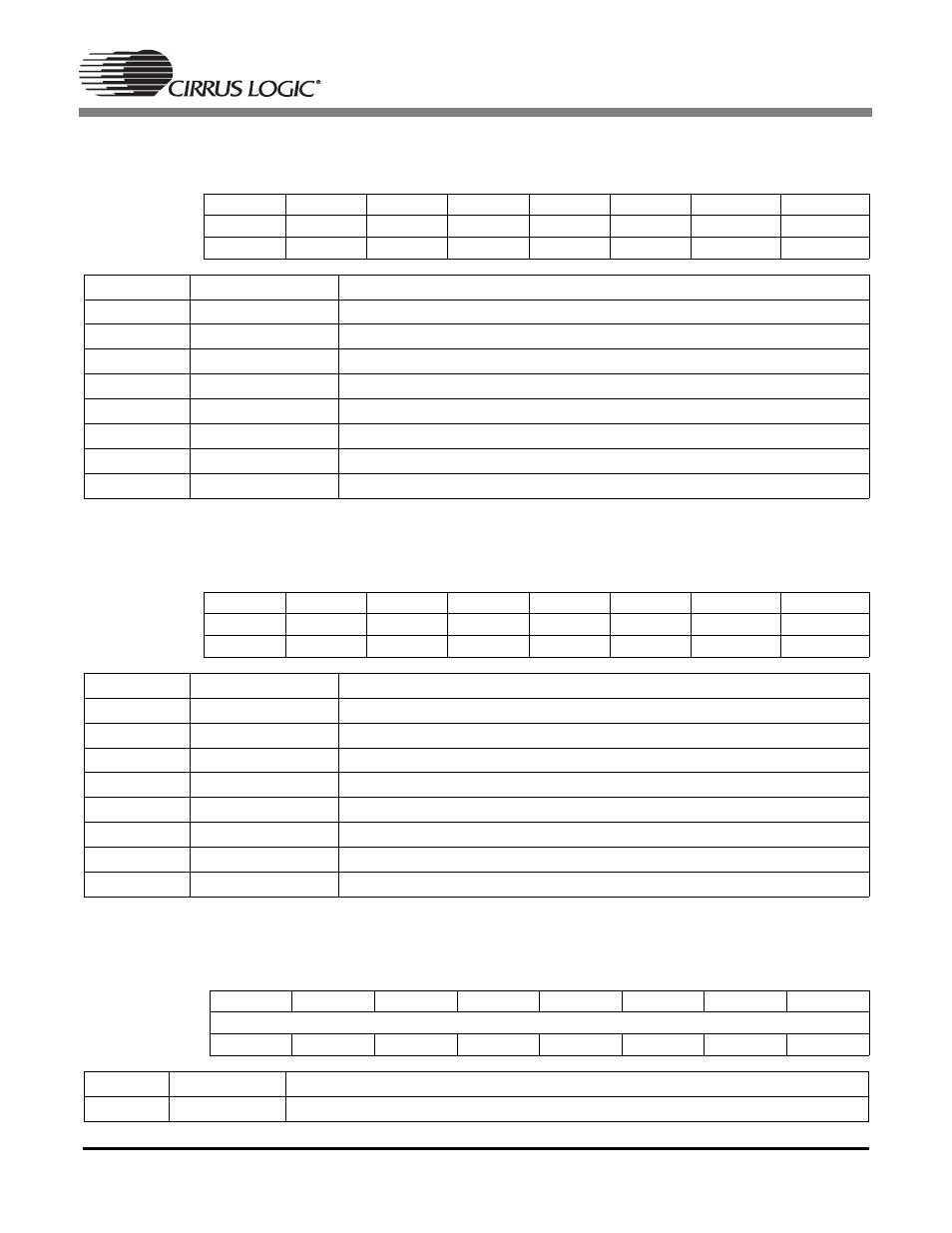
ide Screen Signalling Register 1
Address
0
×
1F
WSS_REG_1 Read/Write
Default Value = 00h
Wide Screen Signalling Register 2
Address
0
×
20
WSS_REG_2 Read/Write
Default Value = 00h
F
ilter Register 0
Address
0
×
22
CB_AMP
Read/Write
Default Value = 80h
Bit Number
7
6
5
4
3
2
1
0
Bit Name
WSS_15
WSS_14
WSS_13
WSS_12
WSS_11
WSS_10
WSS_9
WSS_8
Default
0
0
0
0
0
0
0
0
Bit
Mnemonic
Function
7
WSS_15
PAL: group 2, bit 7, NTSC: bit 16
6
WSS_14
PAL: group 2, bit 6, NTSC: bit 15
5
WSS_13
PAL: group 2, bit 5, NTSC: bit 14
4
WSS_12
PAL: group 2, bit 4, NTSC: bit 13
3
WSS_11
PAL: group 1, bit 3, NTSC: bit 12
2
WSS_10
PAL: group 1, bit 2, NTSC: bit 11
1
WSS_9
PAL: group 1, bit 1, NTSC: bit 10
0
WSS_8
PAL: group 1, bit 0, NTSC: bit 9
Bit Number
7
6
5
4
3
2
1
0
Bit Name
WSS_7
WSS_6
WSS_5
WSS_4
WSS_3
WSS_2
WSS_1
WSS_0
Default
0
0
0
0
0
0
0
0
Bit
Mnemonic
Function
7
WSS_7
PAL: don’t care, NTSC: bit 8
6
WSS_6
PAL: don’t care, NTSC: bit 7
5
WSS_5
PAL: don’t care, NTSC: bit 6
4
WSS_4
PAL: don’t care, NTSC: bit 5
3
WSS_3
PAL: don’t care, NTSC: bit 4
2
WSS_2
PAL: don’t care, NTSC: bit 3
1
WSS_1
PAL: don’t care, NTSC: bit 2
0
WSS_0
PAL: don’t care, NTSC: bit 1
Bit Number
7
6
5
4
3
2
1
0
Bit Name
U_AMP
Default
1
0
0
0
0
0
0
0
Bit
Mnemonic
Function
7:0
U_AMP
U(Cb) amplitude coefficient