Control register 0, Control register 1 – Cirrus Logic CS4955 User Manual
Page 38
CS4954 CS4955
38
DS278F6
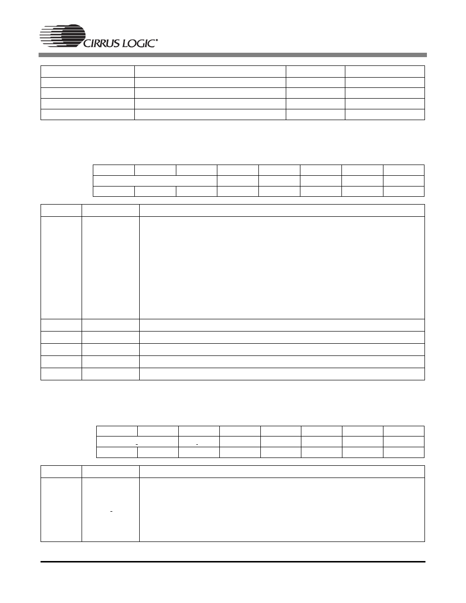
Control Register 0
Address
0
×
00
CONTROL_0
Read/Write
Default Value = 01h
Control Register 1
Address
0
×
01
CONTROL_1
Read/Write
Default Value = 02h
0
×
34
STATUS_0
read only
0
Ч
35 - 0
Ч
59
RESERVED
0
×
5A
STATUS_1
read only
04h
0
Ч
61 - 0
Ч
7F
RESERVED
Bit Number
7
6
5
4
3
2
1
0
Bit Name
TV_FMT
MSTR
CCIR656
PROG
IN_MODE
CBCR_UV
Default
0
0
0
0
0
0
0
1
Bit
Mnemonic
Function
7:5
TV_FMT
selects the TV display format
000:
NTSC-M CCIR601 timing (default)
001:
NTSC-M RS170A timing
010:
PAL-B, D, G, H, I
011:
PAL-M
100:
PAL-N (Argentina)
101:
PAL-N (non Argentina)
110-111:
reserved
4
MSTR
1 = Master Mode, 0 = Slave Mode
3
CCIR656
video input is in ITU R.BT656 format with embedded EAV and SAV (0 = off, 1 = on)
2
PROG
Progressive scanning enable (enable = 1)
1
IN_MODE
Input select (0 = solid background, 1 = use V [7:0] data)
0
CBCR_UV
enable YCbCr to YUV conversion (1 = enable, 0 = disable)
Bit Number
7
6
5
4
3
2
1
0
Bit Name
LUM DEL
CH BW
LPF_ON
RGB_BW
FLD
PED
CBCRSEL
Default
0
0
0
0
0
0
1
0
Bit
Mnemonic
Function
7:6
LUM DEL
luma delay on the composite1 output
00:
no delay (default)
01:
1 pixel clock delay
10:
2 pixel clock delay
11:
3 pixel clock delay
Address
Register Name
Type
Default value
Table 9. Control Registers (Continued)