2 video timing, 1 slave mode input interface, 2 master mode input interface – Cirrus Logic CS4955 User Manual
Page 16: Video timing, 2 video timing 5.2.1 slave mode input interface
CS4954 CS4955
16
DS278F6
5.2
Video Timing
5.2.1 Slave Mode Input Interface
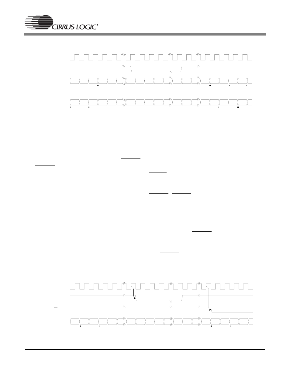
In Slave ITU R.BT601 (not ITU-R.BT656 input)
Mode, the CS4954/5 receives signals on VSYNC
and HSYNC as inputs. Slave Mode is the default
following RESET and is changed to Master Mode
via a control register bit (CONTROL_0 [4]). The
CS4954/5 is limited to ITU R.BT601 horizontal
and vertical input timing. All clocking in the
CS4954/5 is generated from the CLK pin. In Slave
Mode, the Sync Generator uses externally provided
horizontal and vertical sync signals to synchronize
the internal timing of the CS4954/5. Video data that
is sent to the CS4954/5 must be synchronized to the
horizontal and vertical sync signals. Figure
illus-
trates horizontal timing for ITU R.BT601 input in
Slave Mode. Note that the CS4954/5 expects to re-
ceive the first active pixel data on clock cycle 245
(NTSC) when CONTROL_2 Register (0x02) bit
SYNC_DLY = 0. When SYNC_DLY = 1, it expects
the first active pixel data on clock cycle 246 (NTSC).
5.2.2 Master Mode Input Interface
The CS4954/5 defaults to Slave Mode following
RESET high but can be switched into Master Mode
via the MSTR bit in the CONTROL_0 Register
(0x00). In Master Mode, the CS4954/5 uses the
VSYNC, HSYNC and FIELD
device pins as out-
puts to schedule the proper external delivery of dig-
ital video into the V [7:0] pins. Figure
illustrates
horizontal timing for the CCIR601 input in Master
Mode.
The timing of the HSYNC output is selectable in
the PROG_HS Registers (0x0D, 0x0E). HSYNC
can be delayed by one full line cycle. The timing of
the VSYNC output is also selectable in the
CLK
1706
active pixel
#720
HSYNC (input)
V[7:0]
(SYNC_DLY=0)
1705
1704
1703
1728
1
2
3
128
129
264
265
266
267
268
1686
1685
1684
1683
1716
1
2
3
128
129
244
245
246
247
248
Y
Cr
Y
Cb
Y
Cr
Y
horizontal blanking
active pixel
#1
active pixel
#2
• • •
• • •
• • •
• • •
• • •
• • •
• • •
NTSC 27MHz Clock Count
PAL 27MHz Clock Count
1702
1682
active pixel
#720
V[7:0]
(SYNC_DLY=1)
Y
Cr
Y
Cb
Y
Cr
horizontal blanking
active pixel
#1
active pixel
#2
Cb
active pixel
#719
Figure 4. ITU R.BT601 Input Slave Mode Horizontal Timing
CLK
1706
active pixel
#720
HSYNC (output)
V[7:0]
1705
1704
1703
1728
1
2
3
128
129
264
265
266
267
268
1686
1685
1684
1683
1716
1
2
3
128
129
244
245
246
247
248
Y
Cr
Y
Cb
Y
Cr
Y
horizontal blanking
active pixel
#1
active pixel
#2
• • •
• • •
• • •
• • •
• • •
• • •
• • •
NTSC 27MHz Clock Count
PAL 27MHz Clock Count
CB (output)
1702
1682
Figure 5. ITU R.BT601 Input Master Mode Horizontal Timing