Pin description – Cirrus Logic CS1631 User Manual
Page 5
CS1630/31
DS954F3
5
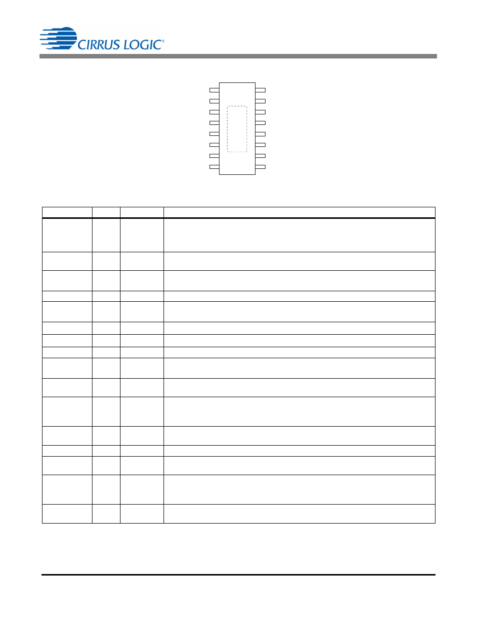
2. PIN DESCRIPTION
Pin Name
Pin #
I/O
Description
BSTAUX
1
IN
Boost Zero-current Detect — Boost Inductor demagnetization sensing input for
zero-current detection (ZCD) information. The pin is connected to the PFC boost
inductor auxiliary winding through an external resistor divider.
IAC
2
IN
Rectifier Voltage Sense — A current proportional to the rectified line voltage is fed
into this pin. The current is measured with an A/D converter.
CLAMP
3
OUT
Voltage Clamp Current Source — Connect to a voltage clamp circuit on the output
of the boost stage.
SGND
4
PWR
Source Ground — Common reference current return for the SOURCE pin.
SOURCE
5
IN
Source Switch — Connected to the source of the boost stage external high-voltage
FET.
SDA
6
I/O
I
2
C™ Data — I
2
C data.
SCL
7
IN
I
2
C™ Clock — I
2
C clock.
NC
8
-
No Connection — Leave pin unconnected.
SYNC
9
OUT
Second Stage Synchronization — A digital synchronization signal that indicates
which channel the controller is signaling for each gate switching period.
eOTP
10
IN
External Overtemperature Protection — Connect an external NTC thermistor to
this pin, allowing the internal A/D converter to sample the change to NTC resistance.
FBSENSE
11
IN
Second Stage Current Sense — The current flowing in the second stage FET is
sensed across a resistor. The resulting voltage is applied to this pin and digitized for
use by the second stage computational logic to determine the FET's duty cycle.
GND
12
PWR
Ground — Common reference. Current return for both the input signal portion of the
IC and the gate driver.
GD
13
OUT
Gate Driver — Gate drive for the second stage power FET.
VDD
14
PWR
IC Supply Voltage — Connect a storage capacitor to this pin to serve as a reservoir for
operating current for the device, including the gate drive current to the power transistor.
FBAUX
15
IN
Second Stage Zero-current Detect — Second stage inductor sensing input. The
pin is connected to the second stage inductor’s auxiliary winding through an external
resistor divider.
BSTOUT
16
IN
Boost Output Voltage Sense — A current proportional to the boost output is fed
into this pin. The current is measured with an A/D converter.
I
2
C Clock
Source Switch
Source Ground
Boost Zero-current Detect
Rectifier Voltage Sense
No Connection
SCL
SDA
I
2
C Data
SOURCE
SGND
BSTAUX
eOTP
FBSENSE
GND
GD
Gate Driver
VDD
IC Supply Voltage
FBAUX
Second Stage Zero-current Detect
BSTOUT
Boost Output Voltage Sense
IAC
CLAMP
Voltage Clamp Current Source
16-lead SOIC
NC
SYNC
7
6
5
4
3
2
1
10
11
12
13
14
15
16
8
9
External Overtemperature Protection
Second Stage Current Sense
Ground
Second Stage Synchronization
Figure 2. CS1630/31